💻 Hardware Series, Part I: CPU
I need to buy a computer, which one is the good one? Intel or AMD? Why is this one 500€ and this other is 1500€? It’s this good to play Fortnite? i7 is better than i5? This one comes with Windows 11. If I buy this new computer, will my Facebook still be there?… If you are in the tech world, maybe someone has ever asked you these kinds of questions, and for social responsibility reasons, you should answer them 🙂.
I decided to collect all my notes and discoveries on hardware over the years, and write this Hardware Series to answer these questions.
Hardware Series:
👋 Intro
Since childhood, I’ve been building and fixing computers for friends and family. My high school gaming years were invested chasing higher FPS and lower temperatures, while university deepened my understanding of internal architecture and programming. Now, as Software Engineer, my relation with hardware has evolved to focus on real-world system performance and efficiency.
⚠️Disclaimer: I’m not a hardware expert, so I tried to include all the relevant sources and useful links. 🙂
📃 Content:
- 🕵️ What is a CPU?
- 🛠️ How a CPU Works?
- 🏭 How a CPU is built: Manufacturing process
- 🧠 CPU Cores
- 🔢 Microarchitecture
- ⏱️ Clock speed (GHz)
- 🚀 CPU Cache
- ⚡ Power consumption
- 🔌 Socket
- 🎨 Integrated Graphics
- 🤖 NPUs
- 🆚 How to compare CPUs?
🕵️ What is a CPU?
The CPU is the Central Processing Unit, an electronic circuit that executes instructions (arithmetic, logic, data movement, data manipulation, and input/output (I/O) operations, etc.).
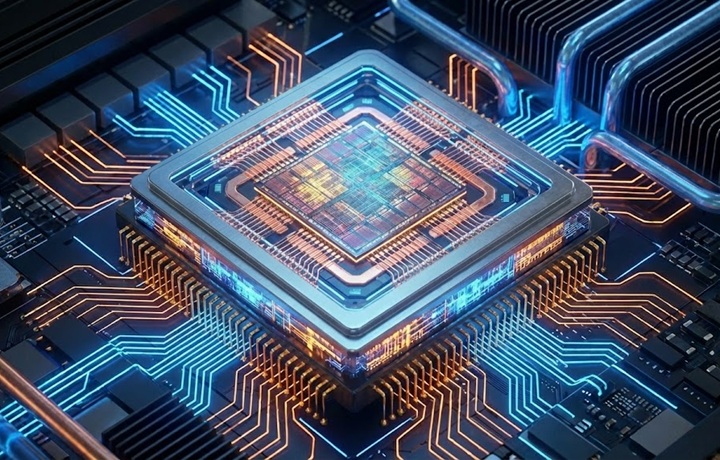
The CPU internals can be represented as the integrated circuit die, known as the chip:
")
Each part of the chip is a different component of the CPU:
")
But in reality, modern processors chips are much more complex. Processors are the result of multiple layers of metal wires stacked and interconnected vertically, on top of a base layer of transistors:
")
If we split the CPU in half (with a hammer 🔨), at microscopic scale we can appreciate the processor’s die and multiple broken layers of wires, and even the transistors’ layer on the background:
, Zoom at 100µm")
Transistors are building blocks of the electronic circuits. A single microprocessor contains billions of transistors
To measure the amount of transistors in a CPU we use transistor density and transistor count. For example:
| CPU | Transistor density | Transistor count |
|---|---|---|
| Intel i9-13900K | 95.08–100.59 million transistors/mm² | 20-26 billion transistors |
| AMD Ryzen 9 9950X3D | 117.78 million transistors/mm² | 20.03 billion transistors |
Branch Education - How do Transistors Build into a CPU? How do Transistors Work ⭐⭐⭐⭐⭐
Modern CPUs primarily use MOSFETs (Metal-Oxide-Semiconductor Field-Effect Transistors). Compared to other kinds of transistors, MOSFETs offer extremely low power consumption, superior scalability for high-density integration, and fast switching speeds, making them the ideal building block for digital logic.

Transistor design has evolved over the years improving density, thermal management, and power efficiency. Some technologies are:
| Technology | Evolution |
|---|---|
| CMOS | Complementary Metal-Oxide-Semiconductor fabrication process. |
| FinFET | Fin Field-Effect Transistor, adding a vertical fin to the structure. |
| RibbonFET | Intel’s implementation of Gate-All-Around technology using ribbon-shaped channels. |
| MBCFET | Multi-Bridge-Channel FET, Samsung’s GAA implementation using nanosheets. |
| GAAFET | Gate-All-Around FET, replacing the vertical fin with stacked “nanosheets”. |
| CFET | Complementary FET, stacking n-type and p-type transistors vertically. |
🛠️ How a CPU Works?
Branch Education - The Engineering that Runs the Digital World How do CPUs Work? ⭐⭐⭐⭐⭐
A computer is essentially a chain of modular layers. Each level simplifies the chaos of the one below, allowing higher-level operations to run without managing low-level details. For example: At the highest level, you are clicking a button; at the lowest, trillions of electrons are moving through silicon.
The CPU is the critical hardware foundation of this chain, acting as the bridge that translates high-level software instructions into the precise electrical switching of billions of transistors.

At the base hardware level, physical transistors act as electronic switches to represent binary states, which are then organized into logic gates to perform fundamental arithmetic. These gates are grouped into a Microarchitecture, creating a specific physical layout of components like the ALU (Arithmetic Logic Unit) and registers that handle data flow. The Instruction Set Architecture (ISA) acts as the critical boundary layer, providing a standardized vocabulary that software can use to communicate with the hardware.
At the software level, compilers and operating systems abstract these low-level instructions into high-level languages, allowing a single line of code to trigger thousands of precise CPU cycles automatically.
🏭 How a CPU is built: Manufacturing process
Branch Education - How are Microchips Made? CPU Manufacturing Process Steps ⭐⭐⭐⭐⭐
The manufacturing process of a CPU consists of many steps: silicon wafer manufacturing, photoresist spin coat, photolithography, photoresist develop, etching, ion implantation, photoresist removal, metal deposition, wafer planarization, oxide deposition, silicon growth, cleaning, inspecting, testing, binning, slicing, packaging, testing, etc.
It’s an iterative process, repeating many steps for each layer. Modern CPUs contain around 80 layers, needing more than 940 steps per chip. The complete process lasts around 3 months.
Some interesting steps are:
1. From Sand to Silicon Wafer
Transistors are semiconductor devices, made by semiconductor materials, primarily silicon, which have some special properties that make it ideal for building transistors:
- Controllable Conductivity: Pure silicon is an insulator. Doping (adding impurities) allows its conductivity to be precisely tuned. This creates the “on” and “off” states needed for digital logic and transistor operation.
- Thermal Stability: Silicon devices maintain their reliable semiconductor properties well across a wide range of temperatures. This stability helps to reduce unwanted leakage current.
- Abundance and Low Cost: Second most abundant element in the Earth’s crust (found in sand) in the form of silicon dioxide (SiO2) or silica.
- Manufacturing Scalability: Can be refined to extremely high purity, so silicon wafer diameters have scaled from 25mm (1960) to 300mm (1999), enabling more dies per wafer.
Everything starts with the right sand, Quartz Sand. Quartz is composed of silicon and oxygen atoms bonded together in a crystalline structure, which is 99.5% silicon dioxide.

Through a process of heating and purification, we can isolate the silicon to produce metallurgical grade silicon with a purity of 98-99%.

To increase the purity further, the metallurgical grade silicon then undergoes a chemical purification process. This involves exposing it to hydrogen chloride gas which reacts with impurities, forming compounds that can be removed. The result is semiconductor grade silicon with 99.99999% (9N) ultra-pure silicon.
Then to preserve atomic alignment and superior semi-conducting properties, a single Boule, Single Crystal Ingot is built.
This Huge crystal is sliced into single-crystal wafers of 300mm diameter. Then they are exhaustively ground, polished, and cleaned.

2. Integrated Circuit Lithography
Lithography or photolithography is essentially a nanoscale photographic process that transfers the circuit blueprint onto the silicon wafer.

Nowadays there are only four microprocessors manufacturers: TSMC, Intel, Samsung and SMIC. To perform semiconductor device fabrication these companies use ASML’s lithography proprietary technologies 🧪, very advanced, complex and expensive machines to perform this step. We can find two different technologies:
Extreme ultraviolet lithography (EUV), 13.5 nm wavelength.
Deep Ultraviolet lithography, 192 to 365 nm wavelength.
The lower the ultraviolet wavelength, the more precision in the chips, so smaller transistors which means more computational capacity. The scale we use to compare this precision is called process node.
3. Process Node (nm)
⚠️ Process Node (nm) is NOT transistor size, it’s a commercial name 😱.
Traditionally, the idea behind this measure was to get an approximation of CPU transistor density. To calculate this we had to measure the transistor’s gate length and project it over the space that a chip fills in the silicon wafer.
In 1965 Gordon Moore, one of the three co-founders of Intel, published an article predicting that by 1975 the quantity of transistors in a chip would double every year.
By 1975 he was right, and wrote another article, and he expected that this tendency will continue at least until 1985, and then we will start finding problems to create much smaller transistors. That’s exactly what happened so now we know this as the Moore’s Law.
During the 60s, 70s, 80s, Gate and Metal Pitch length of the transistors were reduced proportionally, following Moore’s Laws.
Transistor technology structures have changed with the years. Transistor gate and pitch do not evolve proportionally anymore., but the standards continue to use the old nomenclature in honor of Gordon Moore.
Nowadays International Roadmap for Devices and Systems (IRDS), Lithography standards give a table for the real dimensions of process nodes, for example for 7 nm, gate pitch is 54nm and gate length is 20nm. And then, every manufacturer adapt this standard to their production process:
| PN (Standard) | Process name | Company | Gate pitch | fin pitch | T.Density (MTr/mm²) |
|---|---|---|---|---|---|
| 7 nm | 7LPP | Samsung | 54 nm | 27 nm | 95.08–100.59 |
| 7 nm | N7 | TSMC | 57 nm | N/A | 91.2–96.5 |
| 7 nm | Intel 7 | Intel | 60 nm | 34 nm | 60.41–63.64 |
| 7 nm | N+2 | SMIC | 60 nm | Unknown | Unknown |
In the closer future, standards could break the nanometer barrier, we could start using angstroms instead of nanometers.

Notice that 1 single atom of silicon has a diameter of 2.2 angstroms, so it could look like we are getting close to the physical limits of matter 🔬, but as we can see the standard real dimensions are a little bit far away from that, see for example 2 nm, where metal pitch should still be 16nm large.
- The future of TSMC Logic Technology
- The future of Intel Foundry
4. Silicon Lottery
Due to the complexity of the manufacturing process, there are variations between chips. At a microscopic scale, a single particle or photomask defect can damage sections of an integrated circuit.
All chips are tested and categorized or binned (categorized) based on what parts of the integrated circuit still work. In order to reduce waste ♻️, manufacturers decide to shut down parts of the chips, like cores or configure certain frequencies for specific product lines.
❓Could my CPU have hidden cores?
Yes, they could be physically present, but disabled.
For example, based on the number of functional cores or sections, Intel categorizes chips into tiers like i9, i7, i5, and i3, available with or without integrated graphics. Similarly, AMD’s Zen 4 architecture utilizes 8-core Core Complexes (CCX) as modular units, for products requiring fewer cores, some cores are disabled.

Not all fully functional chips behave equally, some chips perform better, support higher temperatures, consume different voltages, or reach higher frequencies.
Manufacturers know this so they categorize the best performing chips into higher categories, as more expensive products, that will perform better. For example: i9 13900K and i9 13900KS, are the same chip but KS is tuned with +0.2GHz. Intel’s K suffix means unlocked, meaning that the CPU can be overclocked.
❓Is there a difference between two i9 13900KS processors?
Yes, some enthusiasts, pre-test CPUs with benchmark programs like Cinebench or Geekbench, to rank CPUs based on performance, power consumption or temperature. For example, extreme overclockers usually search for the best pre-tested CPU, in order to achieve highest frequencies.
❓Do reviewers receive CPU “golden samples” for manufacturers to increase sales?
There is a conspiracy theory on the internet, that manufacturers send the best performing products to the reviewers.
🧠 CPU Cores
A core is the processing unit of a processor, that executes instructions and performs calculations.
Nowadays we use multi-core processors, processors with multiple physical processing units (physical cores). This enables the possibility to execute multiple instructions at the same time, so, more load can be handled, increasing overall speed. Also, programs can benefit from parallel computing techniques if they are implemented at software level.
| CPU | Cores | Threads |
|---|---|---|
| Intel i9-13900K | 24 | 32 |
| AMD Ryzen 9 9950X3D | 16 | 32 |
| AMD Threadripper PRO 9995WX | 96 | 192 |
1. Multithreading
It is the ability of a physical core, managed by the OS, to provide two logical processors that can execute instructions from two different threads during the same clock cycle.
This does not provide the same performance as having 2 physical cores, because depends on whether the tasks have been optimized for multiple threads. For example: (Video Editing, 3D Rendering, Heavy Multi-Tasking) should notice better performance in general, but this increases power consumption and heat output. If this technology is present in the CPU, the number of threads is higher than the number of cores.
Multithreading technology has been implemented by manufacturers with different names, for example:
- Intel’s Hyper-Threading
- AMD’s Simultaneous multithreading (SMT)
❓Should I disable Hyper-Threading to increase fps in games?
Probably not. Nowadays, processor performance and complexity are much higher than in 2002, when this technology came out. Performance impact remains application-dependent, so it will depend if the measured application has been designed taking into account multithreading or not.
Anyways, this technology seems to be disappearing with the usage of big.LITTLE architecture.
2. Hybrid/big.LITTLE architecture

To scale efficiency and performance, modern processors implement big.LITTLE/Hybrid architecture, which consists of having different cores depending on purpose. Intel Core 12th gen or Apple Silicon M Series has imported this technology from smartphones. For example, Intel distinguishes two types of cores:
- Performance-cores (P-cores), High frequency, designed for run heavy single-threaded work, and capable of hyper-threading
- Efficient-cores (E-cores) High CPU efficiency, measured as performance per watt, designed for running background tasks efficiently
❓Does big.LITTLE architecture use AI?
The orchestration between P/E-cores is managed by the kernel’s scheduler, and assisted by the hardware technology: Enhanced Hardware Feedback Interface (EHFI). Intel uses Thread Director, which under the hood analyses hardware telemetry, and processor state and future tasks complexity to do realtime (nanosecond precision) guide the OS scheduler using machine learning.
🔢 Microarchitecture
Microarchitecture (µarch) is the underlying implementation of an instruction set architecture (ISA), it is the physical hardware organization (on the transistor level) of an architecture (for example: CPU, GPU, FPU, DSP, Coprocessor, ASCI, etc.) and how these interconnect and interoperate to implement the ISA.
Here is an example of the Intel Skylake (Gen9 2015) microarchitecture:
")
Also, we can zoom into one single core:

Instruction Set Architecture
Instruction Set Architecture (ISA) is the specification that defines how software interacts with hardware.
An ISA defines the instructions, data types, registers, and the programming interface for managing main memory such as addressing modes, virtual memory, and memory consistency mechanisms. It also includes the input/output model of the programmable interface.
Families of ISAs based on architectural complexity:
| ISA Family | Description | Examples |
|---|---|---|
| CISC | Complex Instruction Set Computer | x86, VAX, System/360, etc. |
| RISC | Reduced Instruction Set Computer | ARM, RISC-V, MIPS, POWER, SPARC, etc. |
| VLIW | Very Long Instruction Word | TMS320, TeraScale, etc. |
| EPIC | Explicitly Parallel Instruction Computing | Intel Itanium |
| MISC | Minimal Instruction Set Computer | Theoretical |
| OISC | One Instruction Set Computer | Theoretical |
Processors with different microarchitectures can share a common instruction set. For example, the Intel Core and AMD Ryzen implement nearly identical versions of the x86 instruction set, but they have radically different internal designs:
Assembly Language
An ISA specifies the behavior implied by machine code, providing binary compatibility between implementations, but machine code is not human-readable.

We can represent this instructions at low level with assembly language, that is the human-readable bridge to machine code.
Here there is an example of a “Hello, World!” program written in assembly language:
section .data
    msg db "Hello, World!", 0x0A  ; The string with a newline (0x0A)
    len equ $ - msg               ; Calculate string length automatically

section .text
    global _start                 ; Entry point for the linker

_start:
    ; --- Step 1: Write to Stdout ---
    mov rax, 1          ; syscall number for 'write'
    mov rdi, 1          ; file descriptor 1 is 'stdout'
    mov rsi, msg        ; address of the string
    mov rdx, len        ; length of the string
    syscall             ; invoke the kernel

    ; --- Step 2: Exit Program ---
    mov rax, 60         ; syscall number for 'exit'
    xor rdi, rdi        ; exit code 0 (success)
    syscall             ; invoke the kernel
And executing it using nasm, in a Linux x86-64 platform:

x86 and x86-64 Architectures

x86, is a complex instruction set architecture with a very rich instruction set. Its license is owned by Intel and only has authorized a few companies like AMD to avoid competition.
It can run complex series of operations in a single clock cycle like multiplication or moving data between places in memory. More transistors are required in the same space. These processors have fast computing power, larger and more expensive chips, with high power consumption. Nowadays, it is the standard in the PC industry.
❓ Where did the 86 come from?
In 1978 Intel released the Intel 8086 microprocessor. It introduced a new architecture with a 16-bit data bus and 16-bit internal registers. While in October 1985 Intel released Intel 80386 (i386) processor, and it introduced a 32-bit architecture with a 32-bit data bus and 32-bit internal registers. This processor series and the next generations *became very popular, so 32-bit computing processors have become called “x86” since this.
This microarchitecture received several revisions over the years to add new features, like virtual memory management, multitasking, protected mode, real mode, or superscalar architecture.
❓ What about x86-64?
In October 1999 AMD announced AMD64, the x86-64 architecture was born as an extension of the x86. This architecture was backward-compatible with the existing software built for the x86 architecture. Introduced 64-bit addressing, 64-bit internal registers, and larger data types. This extension added 64-bit computing to the table and is the most widely used these days in all computers.
Some examples are:
| Manufacturer | Microarchitectures | Process node |
|---|---|---|
| Intel | Golden Cove, Gracemont, Raptor Cove | 10 nm (Intel 7) |
| Intel | Redwood Cove | 7nm, 3nm (Intel 4, Intel 3) |
| Intel | Crestmont | 7nm, 5nm, 3nm (Intel 4, TSMC N6, Intel 3) |
| Intel | Lion Cove | 3 nm (TSMC N3B) |
| Intel | Skymont | 3 nm (TSMC N3B) |
| AMD | Zen 4 | 5 nm (TSMC N6) |
| AMD | Zen 5 | 4 nm, 3 nm (TSMC N4P,N3E) |
ARM Architecture

ARM, is a reduced and optimized set of instructions that were statistically more used. The license is owned by Arm Holdings, authorizing a lot of companies.
All instructions are simple operations using less power. Complex operation complexity was moved to the assembly language at compiler level or replaced by running multiple instructions. These processors have smaller and simpler chips that can be very fast for some types of operations.
ARM designs tend to focus on smaller form factors, battery life, and size, eliminating cooling requirements; that’s why they are mainly used in smartphones.
Every ARM processor has the same hardware architecture and capabilities designed by Arm Ltd. But third-party manufacturers tune these designs, like modifying clock speeds, power limits, and surrounding hardware, to cover different needs and reach market differentiation.
Arm processors are the result of the combination of ARM cores. These cores can be classified by purpose:
- Cortex-A: High performance, systems that run applications for example: Raspberry PI, Smartphones, PCS, Laptops, etc.
- Cortex-R: High response time. Faster than microcontrollers, (For example: used in the car industry).
- Cortex-M: Good power consumption. Designed for embedded systems.
- Cortex-X: High performance peaks. (Like high integer math loads and machine learning).
There are different ARM architecture versions with different instruction sets, for example:
| ARM Architecture | Microarchitectures | Examples |
|---|---|---|
| ARMv8-A | Cortex-A53/A57 | Broadcom BCM2837, Qualcomm Snapdragon 215, Samsung Exynos 7570, 7578, 7580, 7870, 7880, Huawei HiSilicon Kirin Hi1610, Hi1612 |
| ARMv8.2-A | Cortex-A75/A77 | Huawei HiSilicon KIRIN 9000, Qualcomm Snapdragon 670, 710, 712, 845, 850, Samsung Exynos 9820, 9825 |
| ARMv8.5-A | Compatible | Apple M1, A14 |
| ARMv8.6-A | Compatible | Apple M2, M3, A15, A16, A17 |
| ARMv9.0-A | Cortex-A510/A710/A715 | Google Tensor G3, MediaTek Dimensity 9000, Snapdragon 7 Gen 1, Gen 3, Samsung Exynos 2200 |
| ARMv9.2-A | Cortex-A520/A720/A725 | M4, M5, G4, G5, MediaTek Dimensity 9300, 9400 Qualcomm Snapdragon 8 Gen 3, Gen 4, Gen 5, Samsung Exynos 2400, 2500, Xiaomi Xring O1 |
| ARMv9.3-A | Lumex C1-Ultra/Premium/Pro | MediaTek Dimensity 9500 |
❓Are supercomputers using ARM architecture?
Nowadays, 23 of the top 500 supercomputers in the world are ARM-based.
32 and 64-bit Computing

Computing bits refer to the number of bits that the computer operates. As we can see at microarchitecture level, processors circuits operates with very different amounts of bits, like buses, caches, registers (word size), etc.
By operation, we refer to the number of bits a processor uses natively to represent an integer and the number of bits a processor uses to represent a memory address.
- 32-bit computing known as x86, Arm32, i386, i686
- 64-bit computing known as X86-64, x64, AMD64, Intel 64, Arm64
The amount of computing bits define the memory addressing space and the calculation capabilities. For example, operations for very big or very small numbers, can be performed with much fewer instructions if the number of computing bits is higher, because higher numbers can be represented with more bits at the same time.
❓Why we do not use 128-bit processors?
In computer architecture, memory is typically byte-addressable (not word-addressable), meaning each unique memory address refers to a single byte of data (Unit of address resolution).
| Bits | Calculation | Max Addressable Space | |
|---|---|---|---|
| 32-bit | 232 | 4.294.967.296 * 1 byte | 4 GiB |
| 64-bit | 264 | 18.446.744.073.709.551.616 * 1 byte | 16 EiB (16 billion GiB) |
Nowadays, the consensus is that we do not need 128-bit or higher computing yet, because 64-bit memory addressing space for RAM is enough for the max capacity that CPU and motherboard circuits can handle (192GB, 256GB, 2TB, 3TB, 6TB).
But, thanks to certain technologies, we can see that current processors are able to perform operations with much more than 64 bits:
Instruction Set Extensions
Instruction Set Extensions are additional specialized instructions that can increase CPU capabilities like:
| Extension | Description |
|---|---|
| MMX | MultiMedia eXtension. |
| SSE2, SSE3, SSE4.1, SSE4.2, SSE4A | Streaming SIMD (Single instruction multiple data) Extensions for parallelism at instruction level. |
| EM64T | Extended Memory 64 Technology. |
| VT-x / AMD-V | Virtualization extensions. |
| AES | Advanced Encryption Standard hardware acceleration. |
| AVX2, AVX10, AVX512F | Advanced Vector Extensions (256/512 bits) for cryptography, neural networks, and complex calculations. |
| FMA3, FMA4 | Fused Multiply-Add operations (128 and 256 bit) performed in one step. |
| TSX | Transactional Synchronization Extensions for hardware transactional memory support. |
| ARM NEON | Improve multimedia encoding/decoding, user interface, 2D/3D graphics and gaming. |
| SHA256, SHA512 | Hardware acceleration of Secure Hash Algorithm. |
Superscalar
In a Superscalar processor multiple instructions are executed simultaneously in a single clock cycle.
In a traditional instruction cycle (scalar), the CPU performs: Fetch → Decode → Execute. While in a superscalar cycle, the processor: fetches multiple instructions at once, decodes them in parallel, issues them to different execution units (ALUs, FPUs) simultaneously and retires multiple results in a single cycle.
This means that the instruction pipeline has multiple parallel “assembly lines”:

Instruction scheduling optimization is a huge topic, these are some interesting techniques:
| Technique | Description |
|---|---|
| Out-of-Order Execution (OoO) | Allows the CPU to execute instructions as soon as their operands are available, rather than in the original program order. |
| Tomasulo’s algorithm | A hardware algorithm for dynamic scheduling that enables out-of-order execution by using reservation stations to track dependencies. |
| Speculative Execution | The CPU performs tasks that may not be needed to improve performance by staying ahead of the program flow. |
| Branch Prediction | Used to guess the path of a conditional branch before it is known for sure, reducing pipeline stalls. |
| Software pipelining | Used to optimize loops, in a manner that parallels hardware pipelining. |
| Operand forwarding | Routes results directly from the execution unit to dependent instructions, bypassing the register file to reduce pipeline stalls. |
| Scoreboarding | A centralized hardware technique for tracking data dependencies and managing instruction execution to allow out-of-order processing. |
| Register renaming | Maps architectural registers to a larger pool of physical registers to eliminate false data dependencies. |
| Memory disambiguation | Determines whether memory-access instructions target the same address, allowing them to be reordered safely. |
| Very Long Instruction Word (VLIW) | Packs multiple independent operations that can run in parallel into a single large instruction in advance, shifting scheduling complexity to the compiler. |
⏱️ Clock speed (GHz)
Clock speed (rate) is the heartbeat 💓 of a CPU. It measures how many cycles a CPU can perform in one second. A CPU with a higher clock speed can process more instructions per second.

Nowadays clock speed is expressed as frequency measured in Gigahertz (GHz):
| CPU | Frequency | Clock cycles |
|---|---|---|
| Intel i9-14900K | 6.00 GHz | 6.000.000.000/s |
| AMD Ryzen 9 9950X3D | 5.7 GHz | 5.700.000.000/s |
❓ A processor with higher frequency (GHz) is better than another?
Not necessarily. Normally CPUs core operates at a base clock, when performing standard tasks while staying within a safe temperature and power range. For example i9-13900K base frequency is 3.2 GHz. This is not a fixed value, the systems will automatically modify the cores’ clock speed depending on load and temperatures, this is called dynamic frequency scaling. Also, not all cores run at the same frequency in the same moment, this depends on load distribution.
Also, processors can temporarily operate at boost (or turbo) frequency, for example i9-14900K can run up to 6 GHz. This is used for heavy tasks, and increases execution speed, but increases power consumption and heat.
❓ Are processors with the same frequency (GHz) equal?
Not necessarily. The average number of instructions executed for each clock cycle is measured as Instructions Per Cycle (IPC). Modern processors are considered superscalar because they have multiple execution units (ALUs) working in parallel (IPC is around 3-8). This is not a fixed value, but we could consider it the “hidden” power of a CPU.
If we compare a modern processor to one from ten years ago, even if they share the same frequency (GHz) and the same number of cores, the modern CPU will significantly outperform the older one. This is because modern microarchitecture is much more advanced and efficient, leading to a substantially higher IPC.
❓ Who produces clock cycles?
Branch Education - How do Digital and Analog Clocks Work? ⭐⭐⭐⭐⭐
In modern computers, clock cycles are generated by a crystal oscillator. This component uses the natural resonance of a vibrating quartz crystal to create a very precise electrical signal. This oscillator is in the motherboard, and its chip behavior can be programmable and customizable at BIOS level.

The crystal vibrates with incredible precision, at a base frequency, for example 100 MHz, we call this Base Clock (BCLK).
Modern systems implement a clock multiplier, which is a Phase-locked loop (PLL) frequency multiplier circuit. This means that the final frequency delivered to the system is multiplied. We call this CPU Multiplier or CPU Ratio:
| CPU | CPU Base Clock | CPU Ratio | CPU Frequency |
|---|---|---|---|
| Intel i9-14900K | 100 MHz | 32 | 3.2 GHz |
❓ Does the clock signal “power” the CPU?
No, the electricity provided to the CPU, comes from the VRMs at a certain stable voltage. The clock signal is a separate circuit, and its only job is to carry a high/low, voltage signal. But they are synchronized. For example, when the crystal oscillator triggers a high-speed clock cycle, the VRM detect this surge in demand and react (in microseconds) to keep the voltage from dropping.
🚀 CPU Cache
A CPU cache is a small, ultra-fast type of memory located directly inside the processor. This memory stores copies of the data from frequently used main memory (RAM) locations like data and instructions.

CPU cache is organized into levels based on speed and proximity to the processor cores:
| Memory | Latency | Size | Bandwidth | Location |
|---|---|---|---|---|
| Registers | ~0.15 ns (< 1 cpu cycle) | < 10 KB | >1-8 TB/s | Per core |
| L1 Cache | 0.8 ns (~4 cpu cycles) | 64-192 KB | 1-8 TB/s | Per core |
| L2 Cache | 2.4-2.8 ns (~12–14 cpu cycles) | 1-4 MB | 1-2.5 TB/s | Per core or shared between two cores |
| L3 Cache | 8.0-12.0 ns (~40–60 cpu cycles) | 32-512 MB | 400-1200 GB/s | Shared between all cores |
| Main Memory (x1 DDR5 RAM Module) | 60-80 ns (~200-600 cycles) | 8-512 GB | 30-70 GB/s | Outside the CPU |
The CPU checks caches sequentially (L1 → L2 → L3) and only accesses main memory (RAM) if the data is not found in any cache level. L1 and L2 caches run at the same frequency as the processor. While L3 can sometimes run at a different frequency (this can be overclocked separately at BIOS level). CPU Cache hit rate is very high (around 95-97%).
❓ The bigger the cache the better?
Not necessarily. Total cache size (like 96 MB L3) is great for marketing, but latency matters more. Look at cycles-to-hit (Hit Latency) for L1, L2, and L3. Large caches, for example AMD’s 3D V-Cache, significantly reduce DRAM wait states which boost performance for large-dataset simulations or frame-time consistency in gaming.
Some interesting CPU cache technologies are:


| Technology | Description |
|---|---|
| AMD 3D V-Cache | Vertically stacked L3 cache using 3D Hybrid Bonding. Found in X3D processors to increase cache capacity by stacking chips vertically. |
| Intel Ring Bus | Interconnect between cores, the LLC (L3 cache), integrated graphics, and the System Agent. It provides ultra-low latency for consumer tasks but has limited scalability (more cores, more stops in the bus) |
| Intel Mesh | A 2D grid architecture used for servers. Higher bandwidth and more scalable allowing data to take direct paths. Supports many more cores. |
| Intel Smart Cache | Shared cache between L2 on E-cores and dynamic cache for all cores. Allows a single core to utilize the full L2 or L3 cache when others are inactive to reduce cache miss rates. |
| Intel IA Cores L1/L2 | L1 is All-way (instructions + data) associative in both P-Cores and E-Cores. |
⚡ Power consumption
❓ Is TDP power consumption?
No. Manufacturers give us Thermal Design Power (TDP), or Thermal Design Point, measurement expressed in Watts. This metric tells us how much energy over time the CPU theoretically outputs as heat. So, it’s a cooling target metric. The higher the TDP, the better the cooling system should be in order to prevent overheating. For example:
| CPU | TDP |
|---|---|
| Intel Core Ultra 9 285K | 125 W |
| AMD Ryzen 9 9950X3D | 170 W |
| Apple M4 Max (16 cores) | 90 W |
If we want to know the actual power consumption of the CPU, we should look for others specs. For example, AMD’s PPT (Package Power Tracking), which measures the power delivered to the socket. On the other hand, Intel gives us PL1 (Power Limit 1), this is the sustained or average power that the CPU is set to draw, while PL2 (Power Limit 2) is the turbo power that the CPU can draw.
| CPU | PPT | Turbo Boost PL1/PL2 | Turbo Boost PL2 Extreme | Power |
|---|---|---|---|---|
| Intel Core Ultra 9 285K | - | 250 W | 295 W | - |
| AMD Ryzen 9 9950X3D | 230 W | - | - | - |
| Apple M4 Max (16 cores) | - | - | - | 167 W (estimated) |
The voltage supplied to the CPU, is stable voltage (as much clean as possible), delivered by the Voltage regulator modules (VRMs) that transform the 5/12 V coming from the power supply to much lower voltages:
| CPU | Power | Average voltage |
|---|---|---|
| Intel Core Ultra 9 285K | 250 W | 1.121 V |
| AMD Ryzen 9 9950X3D | 230 W | 1.28 – 1.31 V, max: 1.4 V |
Voltage is not linearly related to frequency, but they are interdependent. Each core uses different voltages. More CPU voltage is equal to more heat. Like with clock speed, CPUs use Dynamic voltage scaling, to automatically adjust voltages, depending on load, heat, power consumption, etc.
❓ Can we tune these voltages manually?
Yes, these values can be modified at BIOS level to a certain value or just adding an offset (for example + 0.01 V or - 0.01 V). While tuning we can do Overvolting, that increases stability at higher clock speeds but increases power consumption and heat, reduces lifespan.
🌡️ Temperature
CPUs generally run at a certain temperature (30-80°C), depending on load. Remember that CPUs use dynamic frequency scaling and dynamic voltage scaling, which means that depending on needs, by core, CPUs can automatically adjust frequencies or voltages to reduce heat, save battery, etc.
❓ Can the CPU just burn out? 🔥
Generally not. In case temperatures exceed certain values, typically 90-100°C, the processor immediately lowers its clock speed (GHz) and sometimes its voltage, to prevent it from overheating and suffering permanent damage. This is known as thermal throttling. If the temperature problem persists, the processor will automatically shutdown.
CPU cooling is mandatory:

To keep CPUs from overheating, thermal energy is moved from the chip to a larger surface like a heatsink or radiator via conduction. This heat is then dispersed into the environment using active airflow (fans), liquid circulation, or passive dissipation through the device’s casing (like in smartphones).
🔌 Socket
The CPU die is mounted on a printed circuit board (PCB) that distributes all the connection points to landing pads that interface with the landing grid array (LGA) on the motherboard, the socket. These connection points provide an electrical interface that allows a CPU to communicate with the rest of the computer.
| Type | Description |
|---|---|
| LGA Land Grid Array | Pins are in the motherboard socket (currently used in PCs, Servers) |
| PGA Pin Grid Array | Pins are on the CPU (deprecated) |
| BGA Ball Grid Array | CPU is permanently soldered to the board (Laptops, Smartphones, etc.) |


Each manufacturer has its own sockets, and the number of pins/landing is different. It’s important that the motherboard socket and the CPU match. For desktop PCs, some of them are:
| Socket | Pin count | Processors |
|---|---|---|
| AM4 | 1331 | AMD Ryzen 1000, 2000, 3000, 4000, 5000 |
| sTRX4 | 4094 | AMD Threadripper 3000 |
| LGA 1200 | 1200 | Intel Core 10th, 11th Gen |
| LGA 1700 | 1700 | Intel Core 12th, 13th, 14th Gen |
| sWRX8 | 4094 | AMD Threadripper 5000 |
| AM5 | 1718 | AMD Ryzen 7000, 8000, 9000 |
| sTR5 | 4844 | AMD Threadripper 7000, 9000 |
| LGA 1851 | 1851 | Intel Core Ultra 200S |
Pins are used for power delivery, transmitting data, and every pin is wired to a motherboard bus, like PCI Express, USB, etc. Manufacturers usually leave some pins unused, for future technology implementations. Here are some socket pin maps:

🎨 Integrated Graphics
Modern CPUs often include a built-in integrated graphics processing unit (iGPU). In this configuration, the CPU cores and the iGPU share the same pool of RAM and memory address space. In contrast, dedicated GPUs utilize their own independent processor chip and high-speed video memory (VRAM). The amount of shared memory for an iGPU can often be manually allocated in the BIOS.
❓ Integrated GPUs are much less powerful than dedicated GPUs?
Traditionally iGPUs are generally much less powerful than their dedicated GPUs. However,
in the last two years (2024–2026), the gap has closed significantly, for example Intel Core Ultra or AMD Ryzen AI series can now outperform entry-level dedicated GPUs from just a few years ago while using a fraction of the power. This is why many thin and light laptops no longer come with dedicated graphics cards.
| Laptop CPU | Integrated Graphics | Architecture |
|---|---|---|
| AMD AI 9 HX 370 | Radeon 890M Graphics | RDNA 3.5 |
| AMD Ryzen AI Max+ PRO 395 | Radeon 8060S Graphics | RDNA 3.5 |
| Intel Core Ultra 9 285H | Intel Arc 140T GPU | Xe2-LPG |
| Intel Core Ultra X9 388H | Intel Arc B390 | Xe3-LPG |
| Qualcomm Snapdragon X2 Elite Extreme (X2E-96-100) | Qualcomm Adreno X2-90 | - |
| Apple M4 Max (16-CPU 40-GPU) | Apple M4 Max (40 Core) | - |
🤖 NPUs
We are living in the AI revolution era. And GPUs have evolved so much that the majority of AI algorithms like LLMs can be executed on local machines.
On the other hand, manufacturers are betting on On-Device AI computation inside regular CPU chips using Neural Processing Units (NPU), specialized circuits designed specifically to accelerate AI and machine learning tasks, like blurring in video calls, facial recognition, and voice commands.
To measure how many mathematical calculations (specifically “integer” operations used by AI models) the chip can perform in one second we can use Trillions (tera) of Operations Per Second (TOPS):
| CPU | NPU | TOPS |
|---|---|---|
| AMD Ryzen AI 9 HX 475 | AMD Ryzen AI | 60 TOPS |
| AMD Ryzen AI Max+ PRO 395 | AMD Ryzen AI | 50 TOPS |
| Intel Core Ultra X9 388H | Intel AI Boost | 50 TOPS |
| Qualcomm Snapdragon X2 Elite Extreme (X2E-96-100) | Qualcomm Hexagon | 80 TOPS |
| Apple M4 Max (16-CPU 40-GPU) | Apple Neural Engine | 38 TOPS |
❓Is it better to run AI on a GPU or an NPU?
It depends. GPUs are better for raw speed and power, useful for running large models (LLMs) like Llama 3 or Stable Diffusion locally. While NPUs are better for battery life and background tasks like blurring background in video calls, facial recognition, voice commands, or small assistants.
🆚 How to compare CPUs?
As we have discussed previously, comparing two CPUs based on common specs like number of cores, clock speed (GHz) or cache size is not trivial. The best way to compare CPUs is to check independent reviews online. But in general I will consider:
- Do not trust product specs, like clock speeds and cache sizes (they can be misleading and just marketing). Underlying technologies can have more impact on performance.
- Newer CPU generations will often outperform older ones (Higher Instructions Per Cycle (IPC)).
- Use specialized real-world benchmarks.
- Fit the budget, normally 50% more in cost only gives you 7% more in performance.
- Check for PPT/PL2, when calculating the total capacity of the power supply.
- Check Max memory, Refresh rate, Memory Types, PCI Express lines, ECC support, etc. supported by the CPU, and consider if it’s covering 100% of the theoretical capacity of the motherboard’s chipset.
- If you need hardware acceleration, check for advanced instruction extensions like AVX-512 or ARM NEON.
But it will always depend on your needs, for example when picking a laptop maybe you want the best battery-life saver processor, or when talking about a desktop PC, maybe you need the processor that delivers more fps in games, the most powerful (single thread), the best processor for multitasking, or the one with best smartphone performance, etc.
There are a lot of benchmarks to compare CPUs depending on real-world tasks, and even real-world scenarios like gaming, video editing or 3D rendering.
❓ How do scientists compare CPUs?
They use a variety of metrics like IPC, power and efficiency, latency, etc, but FLOPS (Floating Point Operations Per Second) is the standard. It measures the number of floating-point arithmetic calculations, making it a great metric for Supercomputers, AI and GPU performance, but not so accurate for general-purpose CPU performance, which relies more on Integer operations.