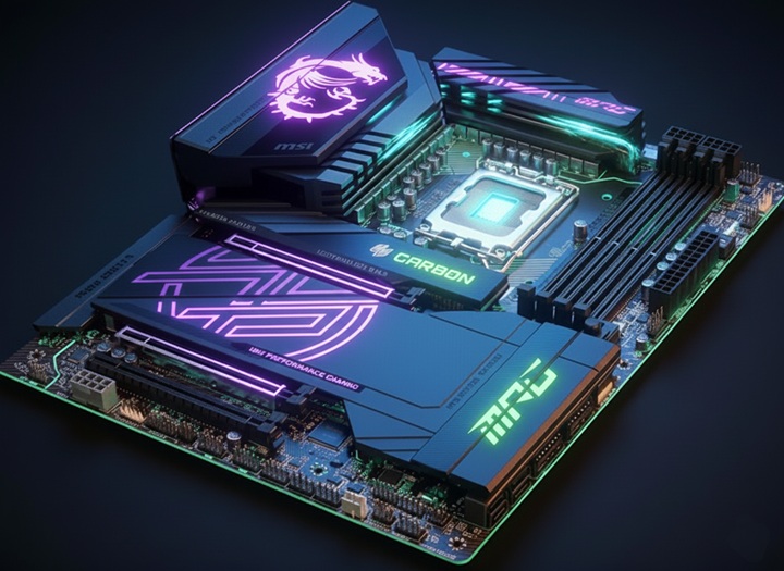
💻 Hardware Series, Part II: Motherboard
We have been building modular PCs “in the same way” since the 80s. If you compare Jeff Atwood’s (Stack Exchange co-founder) PC build blog entries from 2007 and 2020, you will notice that nothing has changed. The process and the components remain the same. But at the same time, everything has changed. All technologies and standards have evolved, but the core concepts remain the same (Processing, Memory, Storage, Expansions, Power, I/O, Graphics).
Modern motherboards still orchestrate all these modular concepts, and today are the result of 40 years of engineering refinement and the operational reality of all humanity.
Hardware Series:
- 💻 Hardware Series, Part I: CPU
- 💻 Hardware Series, Part II: Motherboard
- 💻 Hardware Series, Part III: Memory
⚠️Disclaimer: I’m not a hardware expert, so I tried to include all the relevant sources and useful links. 🙂
📃 Content:
- 🕵️ What is a Motherboard?
- 🎛️ The Chipset
- 📏 Form Factors
- ⚡ VRMs
- 🧠 RAM Slots & Channels
- 🛣️ PCI Express
- 🔌 I/O Panels
- ⚙️ BIOS / UEFI
- 🆚 How to choose a Motherboard?
🕵️ What is a Motherboard?
PowerCert Animated Videos - Motherboards Explained ⭐⭐⭐⭐⭐
Branch Education - How does Computer Hardware Work? - Motherboard ⭐⭐⭐⭐⭐
If the CPU is the brain, the Motherboard is the nervous system. It is the backbone that connects all components, determines expandability, and dictates the lifespan of a build.

The motherboard is the main printed circuit board (PCB). It distributes power and allows communication between the electronic components of a system.

Modern motherboards consist of multiple layers (8 to 16+) of fiberglass, resin, and copper traces. More layers generally mean better signal integrity (less interference between electrical signals) and better durability, which is crucial for high-speed components like PCIe 5.0 lines and DDR5 memory.

❓How thick are copper layers?
Copper Thickness in the US is specified as ounces per square foot (oz/ft2). Greater copper thickness equates to higher current capacity, better thermal management, more power efficiency and more structural resistance, but this increases the cost. Nowadays motherboards usually do 2 oz (600 g/m²) layers but we can find even more in the high-end products.
❓ Who builds Motherboards?
Building a motherboard is a highly automated and manual, multi-stage process generally divided into phases: PCB Fabrication, Surface Mount Technology (SMT), Manual Assembly, Automated optical inspection, and Functional Testing.
The main manufacturers are ASUS, MSI, GIGABYTE, ASRock, and Biostar, but there are many others that build proprietary hardware like Dell, HP, Lenovo, Acer, IBM, etc. Also, we can find other big players for servers like Supermicro, Tyan, or ASRock Rack. These companies design and assemble the motherboards, but they buy and integrate finished components from a large number of third-party suppliers:

For example, they buy chipsets from AMD and Intel, sockets from Lotes and Foxconn, VRMs and MOSFETs from Infineon Technologies, Renesas, or Monolithic Power Systems. PCB components from Zhen Ding Technology, Unimicron, and TTM Technologies. BMC chips from ASPEED Technology. Lattice Semiconductor, Samsung, SK Hynix, & Micron for storage and memory chips that need to be soldered on board, Amphenol & Molex for physical connectors, Murata & TDK for ceramic capacitors, etc.
🎛️ The Chipset
For me this is the second most important thing to check 👀 when building a computer, after the CPU. The Chipset is an integrated circuit that acts as a communication hub and traffic control center between motherboard components. Chipsets determine the motherboard compatibility with external components.
In the past, Chipsets consisted of two main chips: Northbridge, located near the CPU, it handled high-speed communication (RAM, PCIe x16 graphics) and Southbridge, located further away, it managed slower communication I/O like USB, Audio, Storage (SATA/IDE), Networking, and BIOS.
")
On modern motherboards, the Northbridge’s functions are integrated directly into the CPU to reduce latency. The modern Chipset is essentially just the Southbridge, now called the Platform Controller Hub (PCH), handling secondary connectivity like USB ports, SATA drives, WiFi, and extra PCIe lanes.
CPU and Chipset relation defines the maximum theoretical specs of motherboards on a single generation:


PC manufacturers tier their chipsets to segment the market:
| Tier | Intel 800 Series Chipsets | AMD AM5 Chipsets | Features |
|---|---|---|---|
| Enthusiast | Z890 | X870E / X870 | Full CPU/Memory overclocking, maximum PCIe 5.0 lanes, USB4 standard, and multi-GPU support. |
| Mainstream | B860 | B850 | The “sweet spot.” Supports high-speed RAM and PCIe 5.0 for storage. Limited CPU overclocking on Intel. |
| Entry Level | H810 | B840 / A620 | PCIe 4.0 focus, fewer high-speed USB ports, and often limited to two RAM slots. |
We also can have special chipsets for business, for example Intel Chipsets with Intel vPro technology (Q870, W880) offers more stability, remote management and security features at hardware level like: Threat Detection Technology, Boot/BIOS Guard, Total Memory Encryption, remote recovery (even if OS is dead), etc.

Also we have different chipsets for servers (W790, B650E, C621A). But modern server processors like Intel Xeon 6500/6700-series processors can even have Chipset integrated into the processor (For example: ThinkSystem SD650 V4).
❓ How to know CPU/Motherboard/Chipset compatibility?
Chipsets are designed closely with CPU architectures and sockets, so there is a range of compatible processors for each Chipset (generally with the same socket). And a processor can be compatible with multiple Chipsets. So it’s important to know the Motherboard/Chipsets compatibility.
❓ Two boards with the same chipset are equal?
Not necessarily. Like CPUs, not all motherboards’ product lines deliver the same product specs. Two motherboards with the “Z890 chipset” in the product package name can vary in capabilities, for example number of USB ports or PCIe lanes. That’s why motherboards with the same socket/chipset have different prices.
DMI
The Northbridge and Southbridge are connected through PCI Express lanes acting as a high-speed point-to-point link. AMD uses PCIe directly and Infinity Fabric technology, while Intel uses Direct Media Interface (DMI) proprietary technology:
| Version | Transfer Rate | Effective Max Bandwidth |
|---|---|---|
| DMI 1.0 | 2.5 GT/s | ~1 GB/s (x4 link) |
| DMI 2.0 | 5.0 GT/s | ~2 GB/s (x4 link) |
| DMI 3.0 | 8.0 GT/s | ~4 GB/s (x4 link) |
| DMI 4.0 | 16.0 GT/s | ~16 GB/s (x8 link) |
The number of DMI lanes depends on the chipset model used, they can be x4/x8 or even x2 lanes on mobile systems:
| Chipset | DMI Lanes | Bandwidth |
|---|---|---|
| Z790 / Z890 | DMI 4.0 x8 | 16 GB/s |
| B860 / H810 | DMI 4.0 x4 | 8 GB/s |
This is rarely a meaningful bottleneck, but if you run two high-speed NVMe drives through the wrong chipset simultaneously, you may hit a bandwidth ceiling.
📏 Form Factors
The Form Factor is the specification of the printed circuit board (PCB). This specification describes things like: dimensions, power supply type, connectors, location of the mounting holes, number of ports on the back panel, etc. Nowadays, the most common form factors for PCs are:

| Form Factor | Size | Typical Use Case | Expansion Slots (Max) |
|---|---|---|---|
| Extended-ATX | 305 × 330 mm | Enthusiast / Workstation | 8 |
| Standard ATX | 305 × 244 mm | Standard Gaming PC | 7 |
| Micro-ATX (mATX) | 244 × 244 mm | Budget / Compact builds | 4 |
| Mini-ITX (ITX) | 170 × 170 mm | Small Form Factor (SFF) | 1 |
❓Does the size affect performance?
Not necessarily A Mini-ITX board can run an i9 just as fast as an E-ATX board, assuming it has good power delivery (VRMs) and cooling. However, smaller boards have fewer physical slots for RAM (often 1 or 2 instead of 4) and fewer PCIe slots, limiting upgradeability.
In 1995, Intel introduced the Advanced Technology Extended (ATX) motherboard and power supply configuration specification, improving standardization and interchangeability of components. It is the standard that we still use today, but it has evolved with different revisions over the years (I will cover this in depth in a future post), for example:
⚡ VRMs
The Voltage Regulator Module (VRM) converts the 12V coming from your power supply (PSU) down to the ~0.6V - 1.4V the CPU/Cores needs, and it must do this cleanly and stably while the CPU current usage fluctuates wildly (from 10As to 200A in milliseconds).
High-quality VRM is essential to achieving high CPU overclocks, and high stable CPU clocks, since stable clocks require clean and consistent voltage. This is what separates the “cheap” boards from the “quality” boards, even if they have the same chipset.
Also, Motherboards with quality VRMs, can give same Frequency(HZs) using less voltage, generating less heat, than others.

❓How VRMs Work?
The VRM circuit basically lets the electric current pass by opening and closing a switch. Every time the circuit closes, the current passes and we get a pulse. The number of electric pulses in one second determines the Frequency(HZs) of the circuit, so the more Hz, the more pulses in 1 second. This switch is a MOSFET (Metal Oxide Semiconductor Field Effect Transistor). The one connected directly to the 12V source is called High-Side MOSFET.

There are Chokes, which is an electromagnetic coil that transforms the electric current into an electromagnetic field, and slowly sends a remaining lowered voltage to the CPU. Chokes also store energy briefly to prevent sudden dips in power. This low voltage flow is a secondary circuit enabled by a MOSFET known as Low-Side MOSFET.
When High-Side is closed Low-Side is opened and vice versa. The High-Side is only on for 10% of the time, the Low-Side is on for the remaining 90% of the time. Electric current voltage is regulated by modifying pulse length of the MOSFETs. This is done by the Pulse-width modulation (PWM) chip.
There are electrical Capacitors they act like tiny, lightning-fast batteries. They store a charge and release it to fill in the gaps, ensuring the CPU receives a perfectly flat, stable line of power with no ripples or spikes.
There are also diodes and resistors to avoid the current to exceed desired values.
❓What are VRM phases?
Voltage provided by the power supply is not always stable due to micro-variabilities in the electrical network. In order to provide to the CPU the most stable voltage possible, multiple power phases are used and combined in the VRM circuit.
The previous circuit is replicated in multiple phases and current is split in parallel. Pulses are delayed in each phase, handling a portion of the total resulting current. The more power phases a VRM has, theoretically, the better its ability to supply power stably especially in intensive load situations.

Motherboards usually come with 4,6,8 VRMs. Also, the majority of modern motherboards use doublers in order to double the number of VRMs (12,16,24…).

A phase doubler doubles the number of phases by generating two interleaved signals that are formed using the original. Doublers ensure each phase has less load and less stress. This increases VRM durability and supports higher electric loads (more Frequency(HZs)).
❓ What is 8+2 phases?
VRM phases are normally expressed as 8+2, which means 8 phases for the CPU circuit and 2 dedicated to integrated graphics, the memory controller, and the I/O.
❓ More phases is equal to better voltage delivery?
Not necessarily. It could be another marketing trap. High end motherboards generally have more phases, but having more phases doesn’t necessarily mean that output voltage will be more stable or will work at lower temperatures. This is a component where quality almost always beats quantity, so it requires manual testing. Generally Motherboards for overclocking use very good VRMs and usually they cover capacitors with heatsinks.
🧠 RAM Slots & Channels
Linus Tech Tips - How Motherboards Work - Turbo Nerd Edition ⭐⭐⭐⭐⭐
The motherboard provides the physical electrical pathways, (channels) that enable data transfer to the CPU and the rest of the system. These pathways lead to the DIMM slots, which act as the physical interface where memory modules are installed to bridge the gap between storage and processing.
Nowadays, the most common scenario is that boards have 4 DIMM slots and two channels (dual-channel configuration). (I will cover this in detail in a future post).
There are differences in memory speed depending on Motherboards’ channel topology:

| Memory Topology | Description | Best RAM Stick Configuration | Max Frequency Potential |
|---|---|---|---|
| Direct ITX | 1 DIMM slot per channel. Shortest, cleanest traces. | 2 | Highest |
| Daisy Chain | Traces go to the first slot, then extend to the second. Signal is best in the furthest slot. | 2 | High |
| T-Topology | Traces split equally like a “T” to both slots. Signal distance is identical. | 4 | Moderate |
Nowadays, in PC Motherboards Daisy Chain is the standard, prioritizing speed over capacity, while Direct Topology is mainly used in Mini-ITX boards.

On the other hand, servers standard is Fly-by Topology a high-speed routing method, daisy-chaining command, address, control, and clock signals to manage massive amounts of RAM.
🛣️ PCI Express
PCI Express (Peripheral Component Interconnect Express) is the high-speed interface standard used to connect the Motherboard to peripheral devices like GPUs, NVMe SSDs, and network cards. The PCIe Specification is developed and maintained by the PCI Special Interest Group (PCI-SIG). Compared to earlier standards (ISA,PCI, AGP), PCIe supports faster data transfer, uses fewer pins, I/O virtualization, and allows hot swapping.

PCIe uses a point-to-point topology, where every device has its own dedicated connection to the CPU. These connections are made through lanes:

A lane is composed of two differential signaling pairs, with one pair for receiving data and the other for transmitting. Each lane is composed of four wires or signal traces. Conceptually, each lane is used as a full-duplex byte stream, transporting data packets in eight-bit (byte) format simultaneously in both directions. PCIe Link bandwidth is scaled by the number of lanes:
| PCIe Link Lane Width | PCIe 3.0 | PCIe 4.0 | PCIe 5.0 | PCIe 6.0 | PCIe 7.0 | PCIe 8.0 |
|---|---|---|---|---|---|---|
| x1 | 1 GB/s | 1.97 GB/s | 3.94 GB/s | 7.56 GB/s | 15.13 GB/s | 30.25 GB/s |
| x4 | 3.94 GB/s | 7.88 GB/s | 15.75 GB/s | 30.25 GB/s | 60.5 GB/s | 121 GB/s |
| x8 | 7.88 GB/s | 15.75 GB/s | 31.51 GB/s | 60.5 GB/s | 121 GB/s | 242 GB/s |
| x16 | 15.75 GB/s | 31.51 GB/s | 63.02 GB/s | 121 GB/s | 242 GB/s | 484 GB/s |
The PCIe physical pinout has remained identical across all generations enabling universal backward compatibility since 1.0. This means that you can plug a PCIe 5.0 SSD into a PCIe 3.0 Motherboard, and it will still work (but at a slower speed).

We can differentiate two big parts: the keyside (first 22 pins), they handle power (3.3V and 12V), the system management bus (SMBus), and the presence detect signal that tells the system a card is plugged in. On the other hand we have the data lanes used for data transfer.
❓ Can I use a PCIe x4 card in a PCIe x16 Slot?
It’s not the common thing, but if you are in survival mode, yes, it will work. Only the first x4 data lanes will be used, but you will waste the last 12 lanes.
❓ Is the PCIe x16 Slot always a 16 Lanes PCIe?
Not necessarily, many motherboards could have physical x16 slot that is electrically a x4. Normally the ones located more at the bottom. If you plug a high-end GPU into that slot, your software will still run, but you’ll be limited to 1/4th the potential bandwidth.
❓ In which PCIe Slot should I plug the GPU and the NVMe?
To get the higher bandwidth with these components follow the Motherboard’s manual instructions. As seen in the chipset chapter, the top PCIe x16 slot is wired directly to the CPU for the GPU, and normally there are other x4 PCIe Lanes linked between the CPU and the main M2 slot (M2_1, M2_2 or M2_3) slot.
❓ Why are there smaller pins?
Pins “are you present?” PRSNT1 (A1), PRSNT2 (B17, B31, B48 or B81) are shorter, and this is a safety feature called Hot Plug detection. Because they are shorter, they are the last pins to make contact when you plug a card in and the first to break contact when you pull it out. This tells the Motherboard to instantly cut or enable data flow to prevent electrical problems. Also this is essential for servers hot-swapping components.
❓ Can PCIe power supply the whole PCIe card circuit?
Normal cards, yes, but not modern GPUs. Notice that PCIe max power limit is 75W (66W from the 12V rail and 9W from the 3.3V rail) through PCIe Slots. Extra connectors are needed to reach the higher power required for modern CPU chips, GPU memories, and cooling (450-600W) like 12VHPWR.
PCIe Generations
The industry moved to more efficient ways of packing data into the electrical signals, the standard has been evolving and doubling the transfer rates every 3 or 4 years among the different PCIe generations:
| Generation | Release Year | Transfer rate (x1) | Bandwidth (x1) |
|---|---|---|---|
| PCIe 1.0 | 2003 | 2.5 GT/s | 250 MB/s |
| PCIe 2.0 | 2007 | 5 GT/s | 500 MB/s |
| PCIe 3.0 | 2010 | 8 GT/s | 985 MB/s |
| PCIe 4.0 | 2017 | 16 GT/s | 1.97 GB/s |
| PCIe 5.0 | 2019 | 32 GT/s | 3.94 GB/s |
| PCIe 6.0 | 2022 | 64 GT/s | 7.56 GB/s |
| PCIe 7.0 | 2025 | 128 GT/s | 15.13 GB/s |
| PCIe 8.0 | 2028 (planned) | 256 GT/s | 30.25 GB/s |
PCIe 1.0 and 2.0 used 8b/10b encoding, meaning 20% of the bandwidth was wasted on protocol overhead and introduced Non-return-to-zero (NRZ), where basically 1 is represented as a high voltage (+V) and 0 is represented by a low voltage (-V), because the signal doesn’t drop to a neutral state between pulses, it uses the available bandwidth more efficiently than older Return-to-Zero (RZ) methods.
To correct errors the Layer Cyclic Redundancy Check (Link CRC) mechanism is used. Where basically if the checksum of the package fails, the hardware automatically enables a resend package mechanism.
In PCIe 3.0, 4.0, and 5.0: Switched to 128b/130b encoding, reducing overhead to a tiny 1.5%.
PCIe 5.0 operates at much higher frequencies, so the signal needs to be boosted (using Redrivers). At these speeds, signals become incredibly sensitive to noise, so to keep the signal clean, Retimers are used, but they are expensive. Also, more PCB layers are needed, using Low-Loss Materials. This results in much more complex and expensive Motherboards.
PCIe 6.0 introduced Pulse Amplitude Modulation (PAM4 signaling), which allows for even higher densities of data bits (combinations of 2 bits: 10, 11, 01 or 00 instead of 1 bit: 1 or 0 per clock cycle), this is the core concept of future new releases (PCIe 7.0, 8.0).

PAM4 is much more sensitive to noise signals, so it uses forward error correction (FEC). With PAM4 signaling there are four voltage levels into the same space, bit errors are inevitable, bit error rate is much higher at 10-6 (previously 10-12). The solution is a Fixed-Sized FLIT (Flow Control Unit) approach is used: Data is organized into 256-byte packets called FLITs. The transmitter adds a redundant small amount of extra check data to the end of the packet. If a bit flips due to interference, the receiver uses that extra data to mathematically calculate what the bit should have been and corrects it instantly. Also, the previous LCRC mechanism is still working as a second line of defense.

🔌 I/O Panels
Back Panel
This is the main connection hub of the system that allows you to plug in external peripherals, like USB cables, Network, Audio, Monitors, etc.

The most common peripheral interfaces (I will cover this in depth in a future post) that we can find are:
| Feature | Ports |
|---|---|
| Data Transfer | USB4, Thunderbolt, USB Type-C 3.2 Gen 2, USB Type-A 2.0 / 3.2 Gen 1 |
| Networking | Ethernet (LAN), Wi-Fi/Bluetooth Antennas |
| Video Output | HDMI, DP |
| Audio | 3.5mm jacks, 7.1 Audio, Optical S/PDIF, Mic |
| Utility | Buttons for BIOS Flashback, Reset, Safe Boot, Clear CMOS, PS/2 |
Front Panel
The rest of the peripherals connectors will end in other areas of the case, normally on the front or the top of the PC case. These connectors in the Motherboard are usually located in these areas:

In these areas we can find USB Connectors, Audio, Fans, RGB controllers. Also, the Front Panel Connectors(JFP1 or F Panel), this is the cluster of pins that connects your computer case’s On/Off button and LEDs.

⚙️ BIOS / UEFI
PowerCert Animated Videos - BIOS, CMOS, UEFI - What’s the difference? ⭐⭐⭐⭐⭐
In Modern Motherboards BIOS (Basic Input/Output System) is replaced by the UEFI (Unified Extensible Firmware Interface). It’s the first software that runs when the system powers up. It initializes hardware like motherboard’s chipset, memory, and peripherals and hands over control to the Operating system.

In the old days, a Button cell battery (CR2032) was essential for powering CMOS RAM, a tiny bit of volatile memory that stored your BIOS settings (like boot order and CPU clocks). If the battery died, your settings vanished and the system real-time clock (RTC) reset.

Modern Motherboards use pre-wired CR2032. Some Motherboards use Dual BIOS (a primary and a backup) to prevent system failure from corrupted firmware. Also most recent Motherboards can have up to 64MB of BIOS memory, which allows them to store even primary drivers directly in the BIOS.
❓Do I need to update my BIOS?
Depends, for personal use if your system is stable generally you don’t, but if you want to be up to date with security updates, new CPU/Memory support and fix some compatibility bugs, being up to date is highly recommended. In enterprise context, it’s mandatory.
🆚 How to choose a Motherboard?
- Buying a Motherboard means buying a new system. Statistically (I’m 95% sure) you will probably never upgrade any component (like CPU, GPU, NVMe), because when you do a full build, you want to amortize it. Think about how many years you want to amortize the system first.
- Check your peripheral needs first (interfaces, speeds, technology, number of ports, etc.) before starting to look for a Motherboard. Trust me, you will always use more USB ports than you think.
- Look for the CPU and Chipset theoretical max capacity, and then look for the Motherboard that fits your needs (and your budget).
- If you just care about performance, normally a mid-range budget has just a few differences in real performance and temperature compared with high-end motherboards. (Unless you are going to overclock).
- If you spend a lot on a high-performance CPU, do not skimp on quality VRMs. Killing the CPU is not fun.
- If you are doing a low-budget build, just look for the minimum quality requirements and avoid the Marketing traps like built-in screens, RGB lights, 100 VRM phases, etc.
- If you want the fastest load times, prioritize the main storage disk to use PCIe 5.0 directly connected to the CPU.
- How would you interact with the case? Define the position first, having the right peripheral ports accessible from the front/back could be important.
- If you need to avoid cables, look for Motherboards with Bluetooth/WiFi support.
- The Motherboard’s manual is the most important source of knowledge for your computer. If you have doubts between two different boards, just take a look at the manuals and compare.