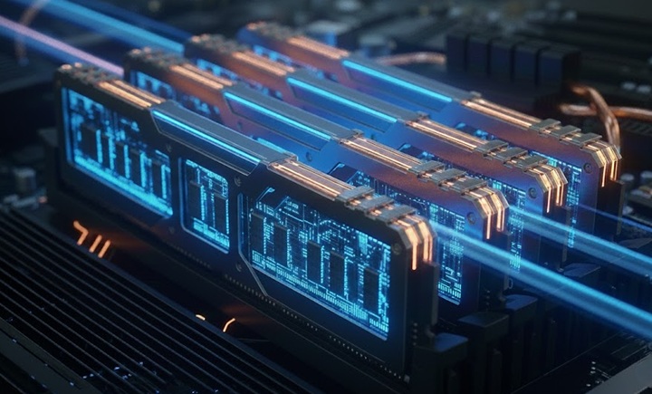
💻 Hardware Series, Part III: Memory
We need more RAM! Probably I have heard this hundreds of times. For some reason people are addicted to vertical scaling-up. And it’s crazy that this is a general solution to many problems (and sometimes it works 😂). But, wait. Do we know what really Computer Memory is? 🤔
Modern Memory is DDR5 SDRAM DIMM. Let’s dive 🕵️ in at what this means.
Hardware Series:
- 💻 Hardware Series, Part I: CPU
- 💻 Hardware Series, Part II: Motherboard
- 💻 Hardware Series, Part III: Memory
⚠️Disclaimer: I’m not a hardware expert, so I tried to include all the relevant sources and useful links. 🙂
📃 Content:
- 🕵️ What is Computer Memory?
- 🔢 SDRAM Memory
- 🧬 DDR Generations
- 🛠️ How Read/Write Works?
- 🏎️ Speed, Bandwidth & Latency
- 🛣️ Channels & Ranks
- 🏭 How Memory is built: Manufacturing process
- 📏 DIMM Variants
- 🌟 CAMM2
- 🤖 HBM
- 🛡️ ECC
- 🔗 CXL (Compute Express Link)
- ⚡ XMP & EXPO
- 🆚 How to choose Memory?
🕵️ What is Memory?
While the CPU executes instructions, Computer Memory is where information is stored for immediate use like data and program instructions. Modern computer memory is also known as Main Memory or RAM (Random Access Memory).

If we take a look at the Von Neumann Architecture (1945), we will notice that the Memory Unit operates with the CPU using different registers:
- MAR (Memory Address Register): Which stores the address of the memory location being accessed.
- MDR (Memory Data Register): Which temporarily holds data being transferred to or from memory.
Nowadays, this behavior is located inside the CPU in the Memory controller (MCC) or Integrated Memory Controller (IMC). Also, it is where all memory tasks take place: Address mapping, buffering, refresh, error corrections, security protocols, scheduling, multi-channel read/write, etc.
🔢 SDRAM Memory
Branch Education - How does Computer Memory Work? ⭐⭐⭐⭐⭐
Nate Gentile - TODO sobre la RAM Parte 2 ⭐⭐⭐⭐⭐
1. DRAM
In 1966, Robert Dennard at IBM invented modern DRAM (Dynamic Random Access Memory) architecture, where just a single transistor and a capacitor can store 1 bit of data. Stacking this very simple circuit allowed much more memory density than previous technologies like Magnetic Core Memory, Drum memory, or SRAM (Static Random Access Memory).

In DRAM the memory cell circuit contains these elements:
- Transistor: The “gate”, which will enable electrons to enter or exit the capacitor.
- Capacitor: The “battery”, where the bit (0 or 1) is stored.
- Bit line: Is where the information that needs to be stored arrives (when writing) or leaves (when reading).
- Word line: Is where the signal to open/close the gate will arrive, enabling write/read operations.
It’s much more scalable to build cheap and simple chips with billions of simple circuits creating general-purpose memories, stacking (transistor and capacitor pair) as arrays of cells:

2. Dynamic
A charged capacitor represents a 1 and an uncharged one represents a 0. Capacitors naturally leak charge over time. To not “forget” any bit of data, the memory controller reads and rewrites the data to refresh the value. This constant, active process of refreshing the state is why it’s called Dynamic.
This is the concept: Memory is accessed many times (billions of times per second) while it is refreshed (thousands of times per second). During refresh time, memory is not available (it is “locked”) 🚨:
")
In reality, memory is refreshed by banks. During this time, the whole bank is not available and all banks are refreshed at the same time, so the whole memory is locked.
This refresh time is standardized by JEDEC and defined as Refresh Interval (tREFI). It tells us how often the memory controller sends a refresh command:
| DDR Gen | Refresh Interval (tREFI) | Refresh Cycle Time (tRFC) | Total Refresh Period (tREF) |
|---|---|---|---|
| DDR1 | 7.8 µs | 70 ns – 120 ns | 64 ms |
| DDR2 | 7.8 µs | 75 ns – 127.5 ns | 64 ms |
| DDR3 | 7.8 µs | 90 ns – 350 ns | 64 ms |
| DDR4 | 7.8 µs | 160 ns – 550 ns | 64 ms |
| DDR5 | 3.9 µs | 295 ns – 410 ns | 32 ms |
❓ Is full memory always locked during refreshing?
Depends. In DDR4, the concept of Fine-Grained Refresh (FGR) was introduced, which makes the duration of lockouts shorter by adjusting tRFC and increasing the refresh rate in 2x or 4x modes. If capacitors are refreshed more often, fewer electrons are needed in every recharge, so lockouts are much shorter.
In DDR5 and LPDDR2 memories, the huge amount of cells makes the 7.8 µs interval inefficient. JEDEC introduced Same-Bank Refresh (REFsb), which allows the controller to refresh one bank while others remain available for data, reducing refresh latency compared with the all-banks memory lockout.
❓ Is refresh time always the same?
No. For example, if memory temperature is high (more than 85°C), the refresh interval is typically halved (for example, to 3.9 µs for DDR4), because capacitors leak charge faster when hot 🔥.
❓ Does SRAM need to be refreshed?
No. As long as the power is on, the state of the transistors remains static, so they have much lower access time. But the circuits are complex and expensive. SRAM is mainly used to build L1, L2, and L3 caches inside CPUs.
3. Synchronous
DRAM is also called Synchronous dynamic random-access memory (SDRAM). It means that the memory chip’s operations are timed (synchronized) to the CPU system clock. The first SDRAM chip was manufactured by Samsung in 1992.

This makes the memory timing predictable, allowing, for example, memory burst mode or CPU out-of-order execution.
❓ Is a 5 GHz CPU synchronized with a 6000 MT/s RAM?
Yes. They are synchronous, but they are not running at the same speed:
- CPU core clock speed is the result of an original Base Clock (BCLK) multiplied by a CPU clock multiplier (100 MHz * 50 = 5 GHz).
- Memory Clock (mCLK) or I/O Bus Clock is the result of the BCLK multiplied by a RAM clock multiplier (100 MHz * 30 = 3000 MHz).
- Memory Controller Clock (uCLK) is the mCLK divided by a ratio (3000 MHz 2:1 = 1500 MHz).
They all come from the same BCLK, so the timing remains predictable.
❓ Can we manipulate the Memory Controller Clock?
Memory Controller Clock speed is a trade-off between memory bandwidth and latency. If memory is much faster than the uCLK, the bandwidth is much higher, but it can cause a bottleneck and create latency 🐌. And if the memory frequency is slower than the uCLK, the bandwidth is much lower, but the latency is minimal 🏎️.
In Intel processors, we can modify Gear Mode in the BIOS (Gear 1, 2 and 4). In AMD processors, this is called UCLK DIV1/2. This technology enables support for faster memory while still maintaining system reliability:
| Gear Mode | Memory Controller Clock (uCLK) | Memory Clock (mCLK) | Transfer Rate |
|---|---|---|---|
| Gear 1 (1:1) | 1800 MHz | 1800 MHz | 3600 MT/s |
| Gear 2 (2:1) | 1500 MHz | 3000 MHz | 6000 MT/s |
| Gear 4 (4:1) | 1125 MHz | 4500 MHz | 9000 MT/s |
Memory Controller efficiency is application dependent. For example, in FPS games it may be more important to have the lowest latency 🏎️, while for 3D editing or loading a high amount of data it is better to have the highest bandwidth 🐌.
4. Random Access
DRAM memory is commonly called Random-access memory (RAM) because when doing reading or writing operations, no matter in which physical memory location (any “random” location), all location positions have the same access time.
This results in a very efficient way to access data, compared with sequential access used in previous technologies. The secret behind this is the Memory Addressing architecture:
Memory Addressing

As we saw in the previous post, the memory controller in the CPU communicates with main memory using the motherboard’s physical Channels. Each memory DIMM stick contains two ranks of memory chips (one on each side of the stick). Every memory chip contains multiple banks. And these banks are arrays of memory cells.
 Memory")
To read a single byte in an 8GB DDR4 memory, we will point to a specific memory address, for example 0x2BF2200D0:

If we take a look at the JEDEC standard addressing, we will see that 0x2BF2200D0 (10 1011 1111 0010 0010 0000 0000 1101 0000 in binary) maps to the following memory address:
| Field | Bit Range / Pins | Binary Equivalent | Value (Decimal) |
|---|---|---|---|
| Row | 16 bit / A[0:15] | 1010 1111 1100 1000 | 45000 |
| Column | 10 bit / A[0:9] | 10 0000 0000 | 512 |
| Bank Group | 2 bit / BG[0:1] | 11 | 3 |
| Bank | 2 bit / BA[0:1] | 01 | 1 |
| Rank | 1 bit / CS_n/C[0:1] | 0 | 0 |
| Byte Offset | 3 bit (not sent by the MC) | 000 | 0 |
The path that needs to be followed is: Channel A => Rank 0 => Bank Group 3 => Bank 1 => Row 45000 => Column 512. This is ultra-fast, because we do not need to find it, just recover data with direct access.
In reality, if we run a read command to this address, we will actually read 64 bits (8 bytes) (or 72 if the memory has ECC), because DDR4 works with 64 data lanes (in this case x8 DQ[7:0] lanes per chip). The memory controller talks to all x8 chips in the rank simultaneously.
🧬 DDR Generations
Modern memory standard is Double Data Rate (DDR), which means it transfers data on both the rising (upbeat) and falling edges (downbeat) of the clock signal, effectively doubling the bandwidth by transferring data twice per clock cycle:

Every few years, a new generation is released, offering higher speeds, higher transfer rate, lower power consumption, and higher capacity:
| SDRAM Name | Release Year | Fastest Standard (theoretical) | Module | Bandwidth (64-bit bus) | Voltage | Max Size Stick PC | Max Size Stick Server |
|---|---|---|---|---|---|---|---|
| DDR | 1998 | DDR-400 | PC-3200 | 3.2 GB/s | 2.6 V | 1 GB | 4 GB |
| DDR2 | 2003 | DDR2-1066 | PC2-8500 | 8.5 GB/s | 1.8 V | 4 GB | 8 GB |
| DDR3 | 2007 | DDR3-2133 | PC3-17000 | 17 GB/s | 1.5/1.35 V | 8 GB | 64 GB |
| DDR4 | 2014 | DDR4-3200 | PC4-25600 | 25.6 GB/s | 1.2 V | 32 GB | 256 GB |
| DDR5 | 2020 | DDR5-7200 | PC5-57600 | 57.6 GB/s | 1.1 V | 128 GB | 512 GB |
| DDR6 | 2027 (estimated) | DDR6-21000 | PC6-168000 | 134.4 GB/s | ? V | ? GB | ? GB |
❓ Do all buses use DDR?
Depends. DDR SDRAM uses double-data-rate signaling only on the data lines. Address and control signals are still sent to the DRAM once per clock cycle (to be precise, on the rising edge of the clock).
But, some less common DRAM interfaces like LPDDR2, GDDR5, and XDR DRAM send commands and addresses using double-data-rate signaling. DDR5 uses two 7-bit double-data-rate command/address buses (CA) to each DIMM, where a registered clock driver chip converts them into a 14-bit SDR bus to each memory chip.
1. Prefetching Architecture
Another difference between generations is Prefetch Architecture, which is a parallelism technique that enables the memory chips to read or write multiple bits of data in parallel from the memory array.
Also, the Burst Length (BL) has been increased across generations too. This is the number of data units transferred over the data bus in a single continuous stream after one READ command.
| SDRAM Name | Pre-fetch | Burst Length |
|---|---|---|
| DDR | 2n | BL2, BL4, BL8 |
| DDR2 | 4n | BL4, BL8 |
| DDR3 | 8n | BL8 |
| DDR4 | 8n | BL8 |
| DDR5 | 16n | BL16 |
For example, when executing a single READ command in DDR4, every single x8 chip will send 8 bits (BL8) to the Data Bus in exactly 4 cycles (the DDR bus has to send 2 bits per cycle). But the problem is that the memory cells are too slow to give 1 bit every half-cycle for 4 cycles 🔥. (If we push the internal chip circuits too much, it results in overheating and corrupt data).
To solve this, an internal pre-fetching action is executed. The chip’s array does one single slow action, grabbing 8 bits of data simultaneously (8n). Data is pre-fetched into a buffer, and the chip can stream the bits across the wire one by one in perfect synchronization.
❓ Waiting for pre-fetching data slow the Memory performance?
No, in fact it’s a performance boost. Notice that the internal pre-fetching action takes 1 single Internal Memory Clock cycle to complete (for example at 400 MHz). For DDR4 (8n Pre-fetch), the external bus is 4 times faster (1600 MHz). In the time it takes the internal memory chip to do one single burst read, the external I/O Bus Clock / Memory Clock (mCLK) has completed 4 full cycles (8 bits), which is exactly enough time to finish the previous burst and be ready for the next one. This predictive behavior creates a perfect pipeline where data never stops moving ⚡.
2. 📱 LPDDR
Low Power DDR (LPDDR) is a variation designed for mobile devices (phones, thin laptops). It runs at lower voltages to save battery and reduce power consumption, but it is usually soldered directly to the motherboard and cannot be upgraded.
While standard DDR SDRAM uses a 64-bit wide memory bus, LPDDR also permits 16 or 32-bit wide channels.
| LPDDR Name | Release Year | Chip Clock Rate | Bus Clock Rate | Transfer Rate | Max Bandwidth (32-bit bus) | Voltages | Max Capacity (Single Package) |
|---|---|---|---|---|---|---|---|
| LPDDR1 | 2006 | 200 MHz | 200 MHz | 400 MT/s | 1.6 GB/s | 1.8 V | 1 GB |
| LPDDR1E | 2006 | 266 MHz | 266 MHz | 533 MT/s | 2.1 GB/s | 1.8 V | 1 GB |
| LPDDR2 | 2009 | 200 MHz | 400 MHz | 800 MT/s | 3.2 GB/s | 1.2/1.8 V | 4 GB |
| LPDDR2E | 2009 | 266 MHz | 533 MHz | 1067 MT/s | 4.2 GB/s | 1.2/1.8 V | 4 GB |
| LPDDR3 | 2012 | 200 MHz | 800 MHz | 1600 MT/s | 6.4 GB/s | 1.2/1.8 V | 8 GB |
| LPDDR3E | 2012 | 266 MHz | 1067 MHz | 2133 MT/s | 8.5 GB/s | 1.2/1.8 V | 8 GB |
| LPDDR4 | 2014 | 200 MHz | 1600 MHz | 3200 MT/s | 12.8 GB/s | 0.6/1.1/1.8 V | 16 GB |
| LPDDR4X | 2017 | 266 MHz | 2133 MHz | 4267 MT/s | 17 GB/s | 0.6/1.1/1.8 V | 16 GB |
| LPDDR5 | 2019 | 400 MHz | 3200 MHz | 6400 MT/s | 25.6 GB/s | 0.5/1.05/1.8 V | 32 GB |
| LPDDR5X | 2021 | 533 MHz | 4267 MHz | 8533 MT/s | 34.1 GB/s | 0.5/1.05/1.8 V | 32 GB |
| LPDDR6 | 2025 | 450 MHz | 7200 MHz | 14400 MT/s | 57.6 GB/s | ~0.5 V | 64-128 GB |
❓Do servers use LPDDR memory?
Yes. Due to its efficiency and bandwidth capabilities, Low Power DDR Memory has become the preferred SDRAM Main Memory in AI Datacenters, especially in CAMM2 modules.
🛠️ How Read/Write Works?
Read and write operations are a 2-step process. Every operation needs multiple commands on different buses:

READ operation:

The first step is to send an ACT command through the command bus. At the same time, the ROW address to activate is sent on the address bus.
In the second step, a RDA command (Read with Auto-Precharge) is sent. The COLUMN address is sent on the address bus.
After waiting some time (CAS Latency), the signal on the Data Strobe bus (DQS) tells us that the data on the Data bus is valid. Notice that it toggles twice per clock cycle (CK bus), which is why this is Double Data Rate (DDR).
Also notice there are 8 data packets labeled D0 through D7. DRAM is designed to send a “burst” of data for every single read command to improve efficiency. In DDR4 we get a burst of 8 (BL8), which means 8 consecutive transfers across that 64-bit bus. So every READ command returns 64 bytes.
❓ Is it the same in DDR5?
In DDR5, the burst size is doubled to 16 (BL16), but the data bus size is 32 bits per sub-channel. Each subchannel has its own dedicated buses (CMD, ADDR, DQS, DQ). So a single read command still returns 64 bytes.
WRITE operation:

The first step is an ACT command that activates a ROW.
In this example, we write 128 bytes, so we need to use 2 WRITE commands for each “package” of 64 bytes. The first WR targets COLUMN and the second WRA targets COL+8 (no row reactivation needed). WRA deactivates the row after the write completes.
The Data Strobe (DQS) bus starts toggling when the data appears on the Data Bus (DQ). The time we wait for writes is called Write Latency (WL).
🏎️ Speed, Bandwidth & Latency
1. Speed / Transfer Data Rate (MT/s)
Double data rate (DDR) means transferring two data in the same clock cycle. This speed of the memory is called Transfer Data Rate which refers to the number of operations transferring data that occur in each second, measured in MT/s. Manufacturers refer to this spec as the bus speed (all pins at the same time).
Do not confuse with the memory bus Clock Rate, measured in hertz (MHz), which is a unit of cycles per second.
| Standard | Bus Clock Rate | Transfer Data Rate |
|---|---|---|
| DDR-400 | 200 MHz | 400 MT/s |
| DDR2-1066 | 533 MHz | 1067 MT/s |
| DDR3-2133 | 1067 MHz | 2133 MT/s |
| DDR4-3200 | 1600 MHz | 3200 MT/s |
| DDR5-7200 | 200 MHz | 7200 MT/s |
❓Why I See DDR5-6000 MHz on Amazon?
This is just marketing. We can consider Transfer Rate MT/s is the double than Clock Rate MHz. So, some companies use a marketing trick to put Speed in 6000 MHz (which is technically incorrect) instead of 3000 MHz, because bigger numbers sell more, and nowadays seems like an industry standard.
2. Bandwidth (MB/s)
Memory bandwidth is the rate at which data can be read from or stored into a semiconductor memory by a processor. Memory bandwidth is expressed in bytes/second. The memory bus is typically a 64-bit (8 byte) data bus. So if we know the Transfer Data Rate, we can calculate the data rate Bandwidth. For example, for DDR-400 it is 400 MT/s * 8 bytes = 3200 MB/s. JEDEC also created the PC modules nomenclature to identify memory modules by peak bandwidth.
| Standard | Module | Bandwidth |
|---|---|---|
| DDR-400 | PC-3200 | 3200 MB/s |
| DDR2-1066 | PC2-8500 | 8533 MB/s |
| DDR3-2133 | PC3-17000 | 17067 MB/s |
| DDR4-3200 | PC4-25600 | 25600 MB/s |
| DDR5-7200 | PC5-57600 | 57600 MB/s |
3. CAS Latency
During read and write data memory operations there are many memory delays (latencies) involved. Also manufacturers deliver these specs in the format CL40-39-39-79 referring to these latencies:

- CL, is the delay between the READ command (Column Address Strobe), and the moment data is available, is specified in clock cycles (ticks).
- Row Address to Column Address Delay (tRCD): Minimum number of clock cycles between opening a row and accessing columns within it.
- Row Precharge Time (tRP): Minimum number of clock cycles between sending the precharge command, closing any open row and opening the next one.
- Row Active Time (tRAS): Minimum number of clock cycles between a row active command and sending the precharge command.
CL, unlike other latency parameters is a fixed value, not a minimum. This predictable fixed CAS latency, enables that the memory controller can perform Pipelining and Bus Scheduling.
❓ How much is CL in seconds?

Depends on the speeds. We have to consider bus Clock Rate, for example: DDR4-2400 CL17 is 17 clock cycles at 1200 MHz, so real delay in nanoseconds will be: 17/(1200 * 10^6) = 14.17 ns.
CL30 is faster than CL40 (at the same frequency). But, higher speed SDRAM has faster (shorter) cycles, high CL not always mean “slower” in real time:
| Standard | CL | CAS latency |
|---|---|---|
| DDR-400 | 3 | 15.00 ns |
| DDR2-1066 | 7 | 13.125 ns |
| DDR3-2133 | 14 | 13.127 ns |
| DDR4-3200 | 24 | 15.00 ns |
| DDR5-7200 | 34 | 9.44 ns |
❓Is DDR5 slower than DDR4 because timings are higher?
No. Early DDR5 memories had slightly higher real latency than top-tier DDR4, but modern DDR5 kits (6000MT/s CL30) are superior in both bandwidth and latency.
❓What is Command rate (CR)?
Sometimes manufacturers specify a fifth parameter, the Command rate, which is sometimes added (normally 2T or 1T, also written as 2N, 1N or CR2). With 1T the memory controller sends a command, and the DRAM processes it in a single clock cycle (fastest settings). With 2T the DRAM is given an extra clock cycle to “decode” the command before acting on it. This adds much higher stability, the default setting in heavy load scenarios like high capacity configurations (more than 64 GB), servers, or when using all four motherboard slots.
🛣️ Channels & Ranks
1. Dual-Channel
Multi-channel technology enables joining multiple channels as a single logical channel, this doubles the data transfer rate between DRAM and the CPU. This enables the CPU to write and read data from the two modules at the same time. Normal DDR4 Bus is 64 bits, in dual-channel it’s 128 bits.
| Configuration | Channels | DDR4 Bus Size | DDR5 Bus Size | Bandwidth Multiplier |
|---|---|---|---|---|
| Single DIMM | 1 | 64 bit | 2 x 32 bit sub-channels | x1 |
| Dual Channel | 2 | 128 bit | 4 x 32 bit sub-channels | x2 |
| Quad Channel | 4 | 256 bit | 8 x 32 bit sub-channels | x4 |
| Octa Channel | 8 | 512 bit | 16 x 32 bit sub-channels | x8 |
| Dodeca Channel | 12 | 768 bit | 24 x 32 bit sub-channels | x12 |

Motherboards can handle more than one DIMM Stick per channel (or not). In servers we can find CPUs that support 8, 12 or even 16 channels. On the other hand, we can find motherboards with 16 DIMM Slots and just 8 channels.
This concept is called DIMMs Per Channel (DPC) or Slot Per Channel (SPC). In a 1 DPC system each channel has one DIMM Slot, in a 2 DPC two slots, etc. This will be a trade-off between speed and capacity. If all slots are filled, the electrical load on each channel increases. This causes “signal noise.” To stay stable, the CPU’s memory controller will often automatically drop the Memory speed.
Normally, servers that prioritize capacity and throughput over clock speed tend to use more slots at a lower safe speed (for example: Lenovo ThinkSystem SR860 V4 Server). While performance servers go for 1 DPC, where the electrical path is very clean, and this allows the memory controller to run at its maximum rated frequency without stability issues (for example: Lenovo ThinkSystem SC750 V4 Neptune Server).
❓ How to enable Dual-Channel?
In our previous post we talked about the DIMM Slots topology (normally Daisy Chain for Desktop computers). It’s important to follow the motherboard’s instructions to enable Dual-Channel.
❓ Is DDR5 Dual Channel a “better” 128-bit bus than DDR4?
Yes, in DDR5, each memory stick has two subchannels ending in a 4 x 32 bit bus, this increases the level of parallelism. In DDR4, the CPU has to wait for the entire 64-bit bus to be free. When doing dual channel, in DDR4 each 64 bit block is “monolithic”, while in DDR5 Dual Channel, the CPU can operate on four different areas of memory simultaneously at the same time.
2. Ranks Organization
DRAM Memory chips are connected and grouped by DIMM Memory Ranks. There are different organizations based on number of Ranks: Single (1R), Dual (2R), Quad (4R) or Octa (8R), and the number of bits managed for each chip: 4 bits (x4), 8 bits (x8) or 16 bits (x16):

| Organization | Chips per Rank | Total Chips | Data Bus Size (DDR4) | Data Bus Size (DDR5) |
|---|---|---|---|---|
| 1Rx16 | 4 | 4 | 64-bit | 2 x 32-bit |
| 1Rx8 | 8 | 8 | 64-bit | 2 x 32-bit |
| 1Rx4 | 16 | 16 | 64-bit | 2 x 32-bit |
| 2Rx8 | 8 | 16 | 64-bit (x2) | 4 x 32-bit |
| 2Rx4 | 16 | 32 | 64-bit (x2) | 4 x 32-bit |
| 4Rx4 | 16 | 64 | 64-bit (x4) | 8 x 32-bit |
| 8Rx4 | 16 | 128 | 64-bit (x8) | 16 x 32-bit |
❓ More Ranks is better?
Depends. Multi-rank modules allow several open DRAM pages (row) in each Rank (8 pages per Rank). This increases the possibility of getting a hit on an already open row address. The performance gain that can be achieved depends on the application and the memory controller’s ability to take advantage of open pages.
Ranks are selected one at a time through a chip select signal (CS), therefore only one rank is accessible at a time.
But, Multi-rank memory modules use a process called rank interleaving, where the ranks that are not accessed go through their refresh cycles in parallel. This pipelined process reduces memory response time, as soon as the previous rank completes data transmission, the next rank can start its transmission.
Also, memory controllers need additional clock cycles to move from one rank to another, so multi-rank organization adds some I/O latency penalty. But on the other hand, it doubles or quadruples the memory capacity on a module.
❓ More chips is better?
Depends, having more chips to reach the same memory capacity can substantially reduce power consumption. For example 2Rx8 32GB memory modules using 16Gb sticks consume 31% less power than 2Rx4 32GB memory modules using 8Gb sticks♻️, while getting similar performance. This performance per watt gain is important, especially for datacenters.
🏭 How Memory is built: Manufacturing process
DRAM Memory manufacturing can be split into two parts: Memory chips manufacturing and Memory sticks manufacturing:
Linus Tech Tips - I made my own RAM! - Micron Factory Tour ⭐⭐⭐⭐⭐
Kingston Technology - DRAM Module Manufacturing Process ⭐⭐⭐⭐⭐
Now there are 3 main DRAM Memory chips manufacturers that control the market share: Samsung, SK Hynix and Micron:

Memory chips manufacturing is similar to CPU Integrated Circuit Lithography. In this case Memory cells (transistor + capacitor) and connections (bit line/wordline) are built on top of a silicon wafer using multiple steps like: ISO area etch, buried wordlines, bit line contact, storage node contact, capacitor etch, mesh spacer, and capacitor plate formation.
For the last 20 years, the industry has been using 2D 1T1C (1 transistor, 1 capacitor) DRAM. Technologies have been evolving in order to gain more density from 6F2 to 4F2 architecture. But, 2D space is not enough. Manufacturers have been researching and developing (R&D) different 3D stacking solutions in order to build chips with more memory cell capacity. For example Vertical Channel Transistor (VCT), which means that the transistor is flipped, so it stands up vertically allowing much more cells into the same area.


Nowadays all manufacturers are using 10nm Process node for chips:
| Manufacturer | Samsung | SK hynix | Micron |
|---|---|---|---|
| DRAM Process Node | 1c (10 nm) | 1c (10 nm) | 1-Gamma (10 nm) |
❓ Is DRAM also affected by Silicon Lottery?
Yes. Memory chips use lithography, and as we saw in CPU Silicon Lottery, this is something natural. In fact, the latency defined in the modules means that it’s the minimum time to ensure that all chips in the module can run without issues. Probably there are individual chips that can perform much better times but they are capped from the factory. Also, modules with better performance chips will run at higher speed, can even be overclocked, and can be sold at a higher price.
❓ What about the Future?
In the future it’s expected that DRAM Cells use 3D Horizontal Stacking technologies (for example Samsung VS-CAT technology).
Once the chips are built, DRAM sticks manufacturers assemble and tune DRAM Modules. For example: Corsair, Kingston, HP, Acer, Gigabyte, Lenovo, GoodRam, Dell, Transcend, G.Skill, etc. Chips manufacturers can sell their own memory sticks with their brand, or even under specialized consumers brands like Crucial (Stopped due to the RAMmageddon).
❓ What is RAMmageddon?
In 2024, computer memory supply shortage started caused by the IA Revolution. This shortage is driven by a structural reallocation of manufacturing capacity toward high-margin products for artificial intelligence infrastructure (Like HBM4 Memory), creating scarcity in consumer and enterprise PC markets (by the time of writing this, prices have grown x4 or x5).
📏 DIMM Variants
1. DIMM
Memory sticks are Dual In-line Memory Module (DIMM)s. These modules are the physical Printed Circuit Board (PCB) that holds the memory chips. Before the 1990s, Single In-line Memory Modules (SIMMs) were used.
Both would have memory chips on both sides of the stick, but the key difference is that in older memory SIMMs, the pins on both sides were connected, so the maximum amount of bits of the data bus was 32-bit. On a DIMM, the pins on the front and back are independent, allowing for a wider 64-bit data bus to communicate with the CPU with a single stick.
In 1997 Small Outline DIMM (SO-DIMM) was introduced by JEDEC, as a size-reduced version of DIMM for laptops:

Different generations are not interchangeable: neither forward compatible nor backward compatible. To make this difference clear and avoid any confusion, their DIMM modules all have different pin counts and/or different notch positions:
| Form Factor | Size | SDR Pins | DDR Pins | DDR2 Pins | DDR3 Pins | DDR4 Pins | DDR5 Pins |
|---|---|---|---|---|---|---|---|
| DIMM | 133.35 x 30 mm | 168 | 184 | 240 | 240 | 288 | 288 |
| SO-DIMM | 67.6 x 30 mm | 144 | 200 | 200 | 204 | 260 | 262 |
| MicroDIMM | 55 x 30 mm | 144 | 172 | 214 | - | - | - |
❓ Can I use any form factor memory?
No, depending on the form factor that is accepted by the motherboard: desktop PCs, workstations and servers can use DIMM, laptops and small PCs use SO-DIMM and small notebooks used to use MicroDIMM, but now the trend is soldering RAM directly to the motherboard.
2. RDIMM/LRDIMM
The Registered memory or buffered memory, is the one that has a register between the DRAM modules and the CPU memory chip controller (MCC).
Standard DRAM computer memory, do not use a “buffer” between the memory and the CPU. They are also called Unbuffered DIMM (UDIMM). This is good to reach much lower latency and higher frequencies, but the amount of Memory is limited (before the system will become unstable).

Servers, manage terabytes of data across many memory slots (16, 24, 32+), and the electrical strain becomes too much for the CPU to handle alone. Registered DIMM (RDIMM) solves this problem by including a register, the Registered Clock Driver (RCD), that buffers commands and address signals. This allows controlling the electrical load and allowing higher memory capacity and stability.
Also, we could find Load Reduced DIMM (LRDIMM), which goes a step further: They buffer and manage the control signals and the data lines. This minimizes the electrical load significantly, allowing servers to be packed with massive amounts of memory (terabytes) without crashing. While with RDIMM clock frequency can drop as you add more DIMMs to keep the signal clean, LRDIMM allow higher frequencies even with full slots (at least for DDR3 and DDR4 servers).
3DS RDIMM
While a standard RDIMM uses single-die packages, a 3DS RDIMM stacks multiple DRAM chips vertically using Through-Silicon Via (TSV) technology. This allows for massive capacities (like 128GB, 256GB or even more 512 GB) that standard memory simply can’t reach.
3. MRDIMM/MCRDIMM
In 2026, in the middle of the AI datacenter race, the need for more capacity and reaching higher stable frequencies has resulted in two similar approaches for server memories:

Multiplexed Rank DIMM (MRDIMM) (powered by JEDEC, AMD and Micron) or Multiplexed Combined Rank DIMM (MCRDIMM) (powered by Intel and SK hynix) allow data from multiple ranks to be transmitted on the same channel. Essentially, a Multiplexer Data Buffer (MDB) takes the data from both ranks and “multiplexes” it. It converts two 4400MT/s (DDR5 RDIMM) streams into a single 8800MT/s stream to the CPU. This enables doubling the frequency and stick capacities. Some of these memories use Tall Form Factor (TFF) to handle even more memory chips. (Example: Micron 256 GB DDR5-8000 MCRDIMM).
In DDR5 Gen, MRDIMM/MCRDIMM servers overtake LRDIMM when comparing memory max server capacity, transfer rate and latency ending in much more efficient (Performance per Watt), making them the choice for “traditional” datacenters in 2026 for example the Lenovo ThinkSystem SR650 V4 Server, and in AI Datacenters they can be found for example in the SR680a V4 but we can also find other options like directly soldered memory or SOCAMM2.
4. CUDIMM
With the introduction of DDR5, in addition to the DDR5 UDIMM memories for consumer systems, a new memory technology for high performance systems has been introduced: Clocked Unbuffered DIMM (CUDIMM), where a Client Clock Driver (CKD) chip in the stick handles the clock signal. This chip cleans and regenerates the signal locally on the memory, and this is needed for speeds above 6400 MT/s, to avoid signals getting blurred, allowing stable speeds of 8400 MT/s to 10000 MT/s.

There also exists Clocked Small Outline DIMM (CSODIMM) which is the reduced version of this technology over SO-DIMM chips for laptops.
To reach high density and max transfer rate, we can find solutions like MSI 4 Ranks 128GB CUDIMM sticks that use dual CKD to maintain 10000 MT/s over a 256 GB system 🤯.
🌟 CAMM2
Fast memory like DDR5 is very sensitive to the synchrony of signals, a large amount of PCB area needs to be dedicated to carefully length-matched traces. The longer these traces get (even 7 cm for SO-DIMM), the more power they waste, and the harder it is to keep the speed high while keeping the signals intact. Also, the mere presence of a soldered connector (even if there is no memory stick inside), creates signal integrity stubs ⚠️ reducing the bus speed. In the future with DDR6, and higher frequencies, this will be even more critical.
One solution to this problem is to just solder the Memory chips to the motherboard, but memory cannot be upgraded or repaired.

To solve this problem, in 2022 DELL introduced Compression Attached Memory Module (CAMM). Replacing the edge connectors with a land grid array, so more pins can be connected with much shorter traces length (around 50% less distance), allowing the module to run at a lower voltage at higher speeds. Also, the device can be much thinner because there is no need to support 2 or 1 SO-DIMM slots, the sticks (57% thinner) are just placed on top of the motherboards. Also, they can reach higher capacity (around 128GB per stick), stable high frequencies (more than 10,000 MT/s), and lower latency.
There also exists Low Power CAMM2 (LPCAMM2), a flagship memory solution for thin and light laptops which uses Low-power DRAM chips.

In 2023, partnering on DELL’s proprietary framework, JEDEC standardized CAMM2.
This technology is in adoption yet, but we can see them in laptops like the Lenovo ThinkPad P1 Gen 7 or Dell Pro Max 16 Plus, and we can even see motherboards supporting this like the MSI Z790 Project Zero Plus to theoretically reach higher frequencies.
SOCAMM2
In 2026, AI Datacenters are powered by HBM4 memories at GPUs. Meanwhile, CPUs use high speed LPDDR5X memory that is co-packaged “soldered” to server motherboards like the NVIDIA Grace Arm CPU.
But, new servers like the Nvidia Vera CPU are using SOCAMM2 LPDDR5X technology:


🤖 HBM
High Bandwidth Memory (HBM) is a 3D-stacked computer memory used in servers for high-performance computing. Nowadays, it is mainly found in GPUs, but it can also be found with CPUs. It is expensive and difficult to manufacture, but it achieves higher bandwidth than DDR5 or GDDR5 while using less power, in a substantially smaller form factor. This is achieved by stacking DRAM dies, interconnected via through-silicon vias (TSVs) (similar to 3DS RDIMMs) using fine interconnect lines, on top of an extra logic die.

| Type | Release Year | Max Pin Speed | Bus Width | Max Bandwidth (per stack) | Max Capacity (per stack) |
|---|---|---|---|---|---|
| HBM1 | 2013 | 1 Gb/s | 8x128 bit | 128 GB/s | 4 dies × 1 GB = 4 GB |
| HBM2 | 2016 | 2.4 Gb/s | 8x128 bit | 307 GB/s | 8 dies × 1 GB = 8 GB |
| HBM2E | 2019 | 3.6 Gb/s | 8x128 bit | 461 GB/s | 12 dies × 2 GB = 24 GB |
| HBM3 | 2022 | 6.4 Gb/s | 16x64 bit | 819 GB/s | 12 dies × 2 GB = 24 GB |
| HBM3E | 2023 | 9.8 Gb/s | 16x64 bit | 1229 GB/s | 16 dies × 3 GB = 48 GB |
| HBM4 | 2025 | 8 Gb/s | 32x64 bit | 2048 GB/s | 16 dies × 4 GB = 64 GB |
❓ Is the JEDEC standard max speed the real maximum?
No. Like DDR Speed, HBM speed tends to increase over the years with optimizations and improvements, also overlapping with the next generation. For example, we can see Samsung HBM4 Memories with max pin speeds of 11.7-13 Gb/s, well over the 8 Gb/s of the standard. Or HBM4E speeds even before the official spec is published.
The HBM bus width is very wide, allowing huge bandwidth per chip in comparison with other technologies, for example:
| Memory Type | Data Rate | Bus Width | Bandwidth |
|---|---|---|---|
| DDR5 (1 stick) | 8800 MT/s | 64-bit | 64 GB/s |
| GDDR7 (RTX-5090) | 32-48 Gb/s per pin | 512-bit (16 chips) | 1792 GB/s |
| HBM4 (1 chip) | 8 Gb/s per pin | 2048-bit | 2 TB/s |
This memory is a critical strategic resource for AI companies these days. Notice that a single AI supercomputer like NVIDIA Vera Rubin NVL72 uses 72 NVIDIA Rubin GPUs, each one running 288 GB of HBM4 memory (8 stacks of 12-Hi (12 die layers) of 36 GB), resulting in 1.5 PB/s of bandwidth (That is 10 times the whole Internet traffic/s) 🤯
❓ Are all manufacturers building the same HBM chips?
No, all manufacturers are using 10nm Process Node for chips these days. But we can see some differences in the Process Node used for the logic die:
| Manufacturer | DRAM Process Node | HBM4 Core DRAM Die | HBM4 Base (Logic) Die Process |
|---|---|---|---|
| Samsung | 1c (10nm) | 1c DRAM | Samsung 4nm |
| SK hynix | 1c (10nm) | 1c DRAM | TSMC 5nm / 12nm |
| Micron | 1-Gamma (10nm) | 1b DRAM | TSMC 5nm / 12nm |
🛡️ ECC
Galactic Cosmic Rays 🌠 can generate a change of state in one memory bit (for example changing a 0 to a 1). This phenomenon is known as Single-event upset (SEU) where high-energy subatomic particles like ions, protons or neutrons accelerated to nearly the speed of light by massive events like supernovas, black holes strikes a sensitive node in the memory cell, it can deposit enough charge to flip the bit 🤯.

These are soft errors, very difficult to detect because there is no trace. If it was part of a critical system instruction, the program might crash or Blue screen of death.
❓ What happens outside the Earth’s atmosphere?
At high altitude and in space these SEUs are an important topic to consider, because without Earth’s atmosphere to filter out cosmic radiation. They use redundancy, physical radiation-hardening and Smart Software. (For example PowerPC RAD750 built in the Curiosity and Perseverance rovers missions).
❓ Only cosmic rays cause SEUs?
No. This phenomenon can also happen because of an alpha particle from trace impurities in the chip packaging like trace amounts of radioactive elements (like Thorium or Uranium). The first widely recognized radiation-generated error (alpha-strike) was the appearance of random errors in the Intel 4k 2107 DRAM in the late 1970s.
ECC memory
One solution to these problems is ECC memory, which basically uses an ECC (Error Correcting Code) mechanism to detect and fix single-bit errors automatically.
The mechanism is similar to PCIe correction strategies. When data is written, the system calculates a checksum. When data is read, the system recalculates the checksum. If the checksums don’t match, the ECC can detect and fix single-bit errors and detect double-bit errors (SECDED).
Historically this technology has been used in servers. In DDR4 ECC Memory, there is a 9th chip dedicated solely to storing the error-correction bits. The “correction” happens as the data travels between the memory chips and the Memory Controller (72 bits data bus, 64 bits for data 8 bits for ECC).
Due to higher densities and frequencies, all DDR5 memory has On-Die ECC to fix errors inside the chip due to the tiny lithography and high density. Once the data leaves the Memory stick it is no longer protected (x2-32 bits data buses).
Also DDR5 ECC like DDR4 ECC memory it’s “server grade” memory, adds Side-band ECC and use extra correction to protect the communication with the Memory Controller (x2-40 bits data buses, 32 for data and 8 bits for ECC in every channel). Also, DDR5 ECC ranks require 10 chips.
🔗 CXL (Compute Express Link)
CXL Consortium - Introducing the CXL 4.0 Specification Webinar ⭐⭐⭐⭐⭐
Compute Express Link (CXL) is an open standard interconnect for high-speed, high-capacity CPU-to-device and CPU-to-memory connections, designed for high-performance datacenter computers. CXL is built on top of the serial PCIe physical and electrical interface, adding new cache-coherent protocols that allow CPUs, accelerators, and memory devices to share and access memory efficiently.
Created in 2019 by the CXL Consortium (with worldwide very important contributors 👀), it absorbed other competing standards and became the dominant CPU memory interconnect standard:
| CXL Version | Release Year | PCIe Gen | Transfer Rate | Bandwidth ×16 (Full Duplex) |
|---|---|---|---|---|
| CXL 1.0 | 2019 | PCIe 5.0 | 32 GT/s | ~63 GB/s |
| CXL 2.0 | 2020 | PCIe 5.0 | 32 GT/s | ~63 GB/s |
| CXL 3.0 | 2022 | PCIe 6.0 | 64 GT/s | ~121 GB/s |
| CXL 4.0 | 2025 | PCIe 7.0 | 128 GT/s | ~242 GB/s |
❓How do AI Datacenters share memory to increase power?
The CXL transaction layer is composed of three dynamically multiplexed sub-protocols on a single link:
- CXL.io: Based on PCIe, it provides device discovery, enumeration, configuration, DMA, and register I/O access.
- CXL.cache: Allows peripheral devices (like accelerators) to coherently access and cache host CPU memory with low latency.
- CXL.mem: Allows the host CPU to coherently access device-attached memory with load/store commands, for both volatile (RAM) and persistent (flash) storage.
Devices that use CXL.io + CXL.mem (type 3) allow servers to expand memory beyond the physical DIMM slots on the motherboard. Memory pooling enables multiple hosts to dynamically share a pool of CXL-attached memory, where a CXL switch allocates memory segments to different servers on demand. This is a fundamental shift for datacenter architecture, enabling disaggregated memory where compute and memory resources can be scaled independently.
❓ What about latency?
CXL memory controllers typically add around 200 ns of latency compared to local DIMM memory 80 ns. This makes CXL ideal for adding capacity for heavy workloads rather than a replacement for latency-sensitive local memory.
⚡ XMP & EXPO
AMD Extended Profiles for Overclocking (EXPO) and Intel Extreme Memory Profile (XMP) are overclocking profiles that can be loaded from BIOS/UEFI. The BIOS will use a Serial Presence Detect (SPD) chip to configure DRAM to get max speeds, different voltages, or stability.
With XMP 3.0, we can adjust even more voltages like (VDDQ, VDD, VPP). SPD chip is non-volatile memory and since DDR5 the chip was expanded and more profiles can be saved, not only manufacturer-tested settings, but also we can persist our own custom overclocking profiles inside the module 🤯.
🆚 How to choose Memory?
- Check compatibility: Check for CPU and motherboard specs, like max capacity and supported speeds.
- Prioritize Dual-Channel: Always install memory in pairs (for example two 16GB sticks instead of one 32GB stick) to take advantage of dual-channel bandwidth. Check your motherboard manual to use the correct slots.
- Find the Speed/Latency sweet spot: Look for the best balance between Transfer Data Rate (MT/s) and CAS Latency (CL). For example, nowadays DDR5, 6000 MT/s with CL30 is often the target for price-performance.
- Fit the budget: normally 25% more in cost only gives you 3% more in performance.
- Don’t fall for marketing traps: Remember that shops often advertise MT/s as “MHz”. Extreme speeds (like 8000+ MT/s) are very expensive and might not run stably unless your CPU’s memory controller and motherboard can handle them.
- Don’t fall for Gamer RGB marketing traps: Check for real specs and reviews. Especially if you are looking for high performance, check number of ranks, internal latencies not only CL, etc.
- Avoid automatic downclocking: If you are looking for high performance, go for two high-speed sticks over four. When running high speed, more sticks equal less stability and normally the system will automatically downclock the speed.
- Pick the right capacity: 64GB of slightly slower memory will serve you better than 16GB of high-speed Memory that forces your system to swap data to disk. For gaming, 32GB is the modern standard.
- Capacity matters most for heavy loads: If you do 3D rendering, use virtual machines, or do heavy multitasking, having enough capacity (32GB, 64GB, or more) is more important than having highest speed.
- Check the Motherboard’s QVL: Manufacturers publish a Qualified Vendor List (QVL) for their motherboards. Buying memory from this list ensures it has been tested to run at its advertised speeds on a specific board.
- Enable XMP / EXPO: If you need to, like for gaming, remember to enable memory overclocking profiles in the BIOS/UEFI, you paid for it.
- Avoid cache misses: Before you buy more RAM, check if your software is actually utilizing the cache hierarchy correctly 🙂.